

Method and apparatus for improved wafer singulation
a technology of electronic substrates and wafers, applied in laser beam welding apparatus, welding/soldering/cutting articles, manufacturing tools, etc., can solve the problems of laser singulation, low efficiency, increased debris and damage, and disadvantages of through cutting
- Summary
- Abstract
- Description
- Claims
- Application Information
AI Technical Summary
Benefits of technology
Problems solved by technology
Method used
Image

Examples
Embodiment Construction
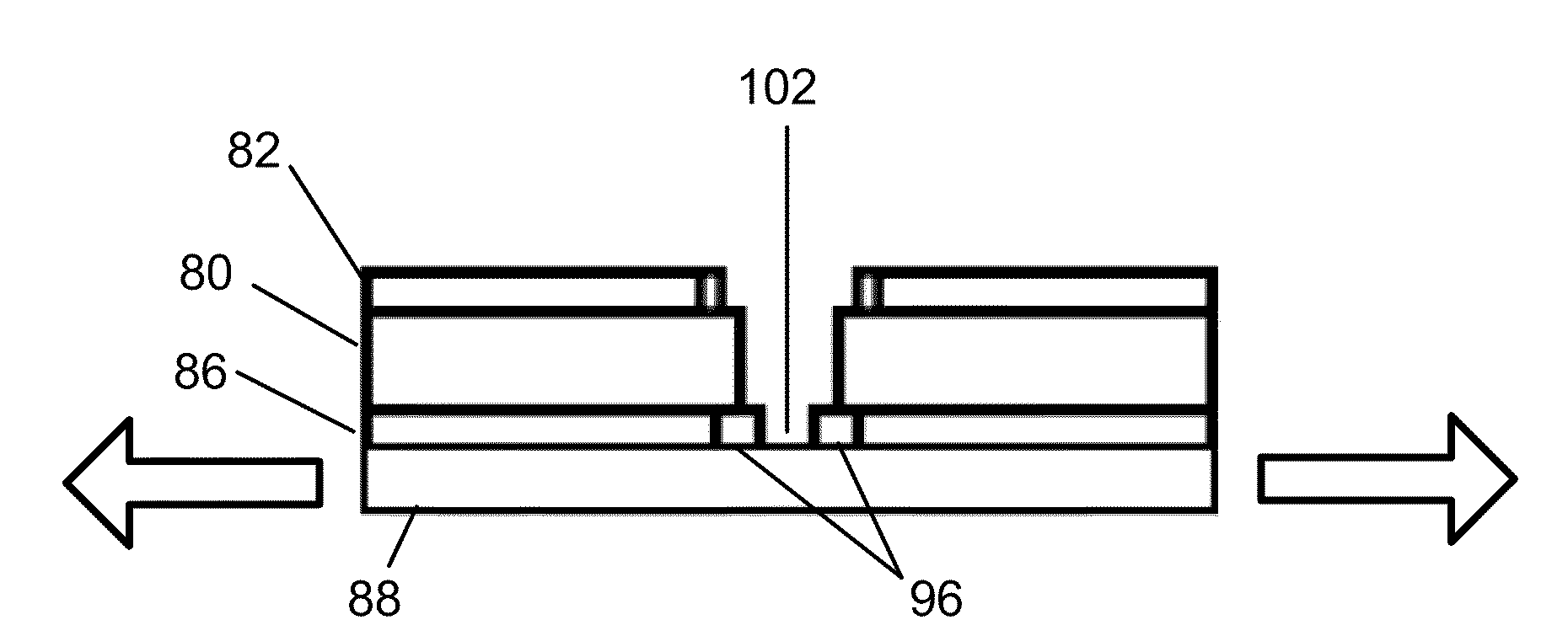
[0024]Embodiments of this invention represent an improved method for singulation of wafers mounted on die attach film (DAF) with a laser processing system. The wafer has predefined streets and a layer of material on the surface opposite the DAF. The laser processing system has first, second, and third lasers having first, second and third laser parameters. A maximum surface texture of the wafer is determined that permits backside removal of the DAF with the second laser using predetermined second laser parameters. First laser parameters are determined that permit the first laser to remove portions of the layer of material from the wafer in a desired region so that substantially all of the layer of material is removed from the desired region and the surface texture of the resulting surface within the desired region is less than said determined maximum surface texture. The first laser is then directed to remove the layer of material from the wafer within a desired area substantially w...
PUM
| Property | Measurement | Unit |
|---|---|---|
| Time | aaaaa | aaaaa |
| Time | aaaaa | aaaaa |
| Time | aaaaa | aaaaa |
Abstract
Description
Claims
Application Information