Methods for manufacturing dielectric films

a dielectric film and film manufacturing technology, applied in the direction of vacuum evaporation coating, transistors, coatings, etc., can solve the problems of plasma damage, sputtering methods, in-plane uniformity, reproducibility, etc., and achieve the effect of reducing the thickness of equivalent oxides

Active Publication Date: 2012-01-26
CANON ANELVA CORP
View PDF6 Cites 23 Cited by
  • Summary
  • Abstract
  • Description
  • Claims
  • Application Information

AI Technical Summary

Benefits of technology

[0046]The invention makes it possible to obtain a dielectric film having (1) a high relative dielectric constant of 40 or more and (2) thermal resistance to high temperature annealing at 1,000° C. According to the invention, therefore, EOT (Equivalent Oxide Thickness) can be reduced by increasing the dielectric constant, even when the method of the invention for manufacturing a dielectric film is applied to a process having high temperature annealing, such as a method for manufacturing a gate insulating film for a CMOS transistor device; a method for manufacturing a blocking insulating film for a MONOS type nonvolatile semiconductor device; or a method for manufacturing an insulating film between a floating electrode and a gate electrode for a FG type nonvolatile semiconductor device.

Problems solved by technology

CVD methods have incubation time in the deposition process and therefore present challenges in achieving film-thickness controllability, in-plane uniformity, and reproducibility.
On the other hand, sputtering methods have the problem of plasma damage or the formation of an interface layer by oxidation of the treated substrate.

Method used


Image

  • Methods for manufacturing dielectric films
  • Methods for manufacturing dielectric films
  • Methods for manufacturing dielectric films

Examples


example 1

Co-Sputtering Example

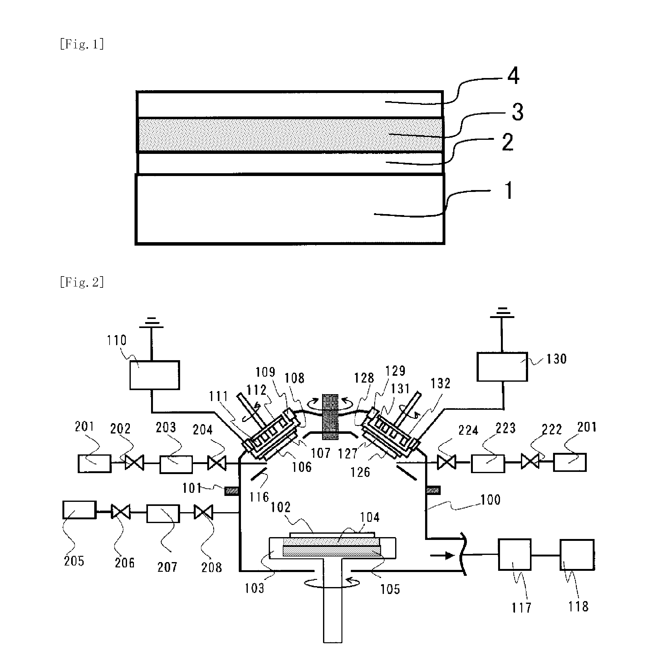
[0117]A first example of the invention is described in detail with reference to the drawings.

[0118]FIG. 14 is a diagram showing a MIS capacitor having a dielectric film formed by the method of the invention. An HfAlO film having an amorphous structure was deposited by sputtering method on a silicon substrate 301 having a silicon oxide film 302 with a thickness of 3 nm to 5 nm at the surface. The targets used were Hf and Al metal targets, and argon, oxygen and nitrogen were used as sputtering gas.

[0119]The substrate temperature, the target power, the sputtering gas pressure, the Ar gas flow rate, and the oxygen gas flow rate may be appropriately determined in the ranges of 27° C. to 600° C., 50 W to 1,000 W, 0.02 Pa to 0.1 Pa, 1 sccm to 200 sccm, and 1 sccm to 100 sccm, respectively.

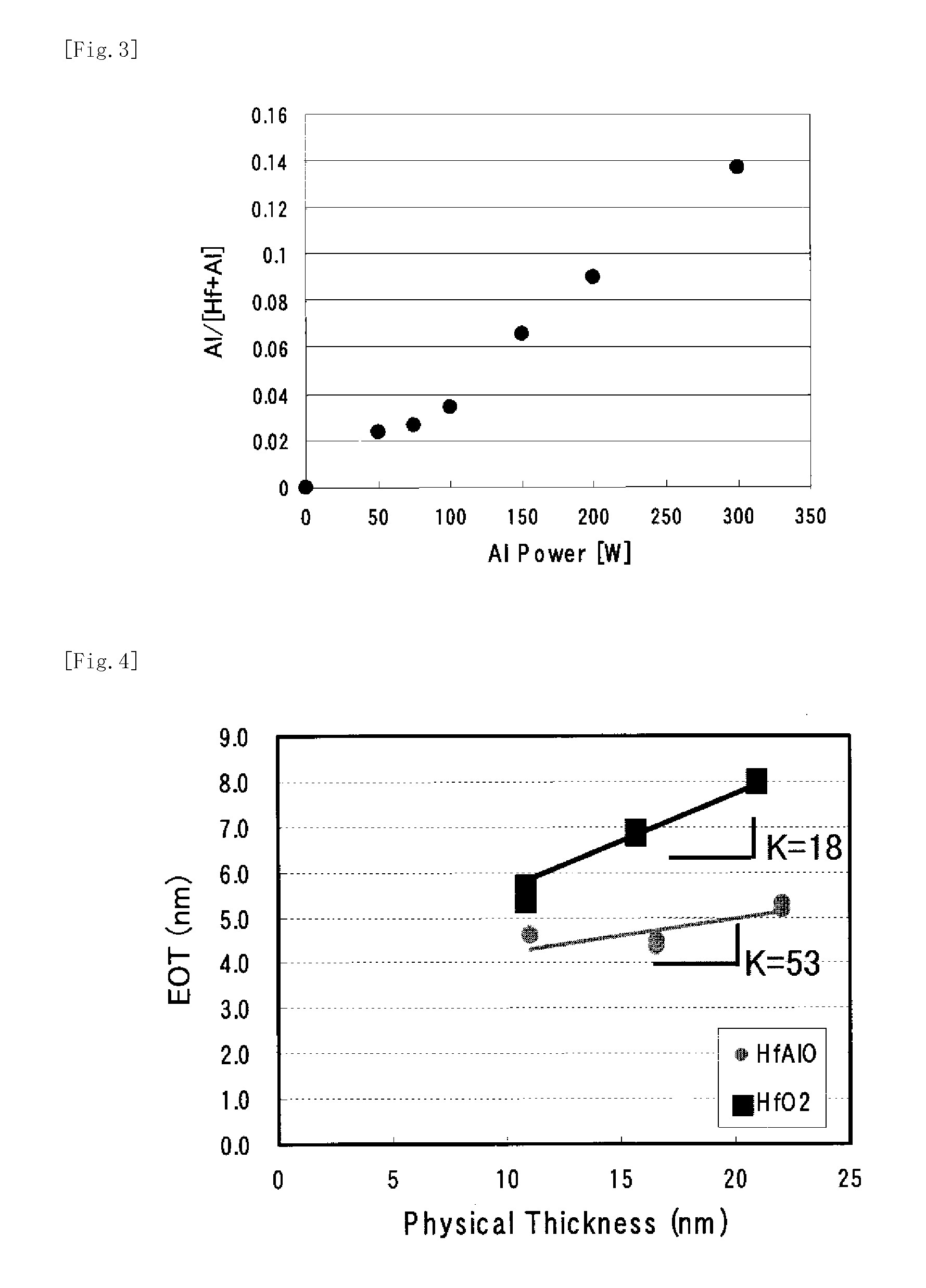
[0120]In this example, the deposition was performed at a substrate temperature of 30° C., a Hf target power of 600 W, an Al target power of 50 W to 500 W, a sputtering gas pressure of...

example 2

Example Applied to Gate Insulating Film

[0134]A second example of the invention is described in detail with reference to the drawings.

[0135]FIGS. 15(a) to 15(c) are diagrams showing the steps of the method of the second example of the invention for manufacturing a semiconductor device.

[0136]As shown in FIG. 15(a), an isolation region 402 was first formed on the surface of a silicon substrate 401 using STI (Shallow Trench Isolation) technique. Subsequently, a silicon oxide film 403 with a thickness of 1.8 nm was formed on the isolated surface of the silicon substrate 401 by thermal oxidation method. An HfAlO film with a thickness in the range of 1 nm to 10 nm was then formed by the same method as in Example 1. Subsequently, the HfAlO film was annealed at 1,000° C. for 10 seconds in a nitrogen atmosphere, so that it was crystallized to form a dielectric film 404.

[0137]A gate electrode 405 of poly-Si with a thickness of 150 nm was then formed on the dielectric film 404. Thereafter, as s...

example 3

Example Applied to Blocking Film of Nonvolatile Memory Device

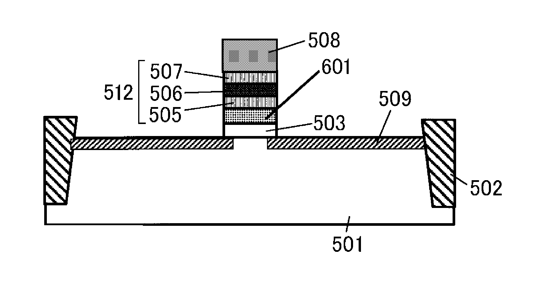
[0141]FIGS. 16(a) to 16(c) are cross-sectional views showing the process of a third example of the invention for the manufacture of a semiconductor device.

[0142]As shown in FIG. 16(a), an isolation region 502 was first formed on the surface of a silicon substrate 501 using STI (Shallow Trench Isolation) technique. Subsequently, a silicon oxide film with a thickness of 30 Å to 100 Å was formed as a first insulating film 503 by thermally-oxidized film method on the isolated surface of the silicon substrate 501. Subsequently, a silicon nitride film with a thickness of 30 Å to 100 Å was formed as a second insulating film 504 by LPCVD (Low Pressure Chemical Vapor Deposition) method. Subsequently, an aluminum oxide film with a thickness of 5 Å to 50 Å was formed as a third insulating film 505. The aluminum oxide film may be formed using MOCVD method, ALD (Atomic Layer Deposition) method, or PVD (Physical Vapor Deposition) method...


PUM

PropertyMeasurementUnit
pressureaaaaaaaaaa
relative dielectric constantaaaaaaaaaa
dielectric constantaaaaaaaaaa

Abstract

A method for manufacturing a dielectric film having a high dielectric constant is provided.
The method is a method for forming, on a substrate, a dielectric film including a metal oxide containing O and elements A and B, wherein the element A comprises Hf or a mixture of Hf and Zr and the element B comprises Al or Si, which includes the steps of: forming a metal oxide having an amorphous structure which has a molar ratio between element A and element B, B/(A+B) of 0.02≦(B/(A+B))≦0.095 and a molar ratio between element A and O, O/A of 1.0<(O/A)<2.0; and annealing the metal oxide having the amorphous structure at 700° C. or more to form a metal oxide containing a crystal phase with a cubic crystal content of 80% or more.

Description

TECHNICAL FIELD[0001]The invention relates to methods and programs for manufacturing a dielectric film and a semiconductor device with the dielectric film.BACKGROUND ART[0002]In the development of semiconductor devices having highly integrated elements, each element is made finer, and the operating voltage is reduced. For example, in the field of MONOS (Metal Oxide Nitride Oxide Semiconductor) type nonvolatile semiconductor devices, as elements are made finer, a blocking film for separating a charge retention layer and a gate electrode is required to have a high dielectric constant. Similarly, in the field of FG (Floating Gate) type nonvolatile semiconductor devices, as elements are made finer, an insulating film between a floating electrode and a gate electrode is required to have a high dielectric constant. In the field of the development of advanced CMOS devices, investigations have been made on a technique of reducing gate-leakage current by using a high dielectric constant mate...

Claims


Application Information

Patent Timeline
Patent Type & Authority Applications(United States)
IPC IPC(8): H01L21/31
CPCC23C14/08H01L29/94C23C14/352H01L21/02145H01L21/02148H01L21/02159H01L21/02161H01L21/02178H01L21/02181H01L21/02189H01L21/02194H01L21/02266H01L21/02356H01L21/28088H01L21/28176H01L21/28194H01L21/28282H01L21/316H01L28/40H01L29/4966H01L29/513H01L29/517H01L29/6659H01L29/7833H01L29/7881H01L29/792C23C14/083H01L29/40117H01L21/28185
Inventor NAKAGAWA, TAKASHIKITANO, NAOMUTATSUMI, TORU
Owner CANON ANELVA CORP
Why Eureka
Try Eureka