Semiconductor device and method of manufacturing the same

a technology of semiconductor devices and semiconductors, applied in semiconductor devices, electrical equipment, transistors, etc., can solve problems such as concern about throughput degradation, change in work function by composition, and increase in the number of processes of producing gate electrodes, so as to suppress the reduction of work functions

Active Publication Date: 2012-02-23
CANON ANELVA CORP
View PDF0 Cites 228 Cited by
  • Summary
  • Abstract
  • Description
  • Claims
  • Application Information

AI Technical Summary

Benefits of technology

[0030]According to this invention, it is possible to suppress reduction of a work function due to diffusion of Si from a polycrystalline silicon layer i

Problems solved by technology

However, the above techniques have the following problems.
The method described in the Patent Document 1 is an effective technique in that TiN having a high work function is realized, and, at the same time, it is possible to suppress the reduction of the work function caused by the diffusion of Si from Poly-Si to TiN in the thermal treatment after the formation of the gate electrode; however, this method does not describe each film composition of TiN, and there is a problem that the work function is change

Method used


Image

  • Semiconductor device and method of manufacturing the same
  • Semiconductor device and method of manufacturing the same
  • Semiconductor device and method of manufacturing the same

Examples


example 1

[0089]A first example of this invention will be described in detail with reference to the drawings.

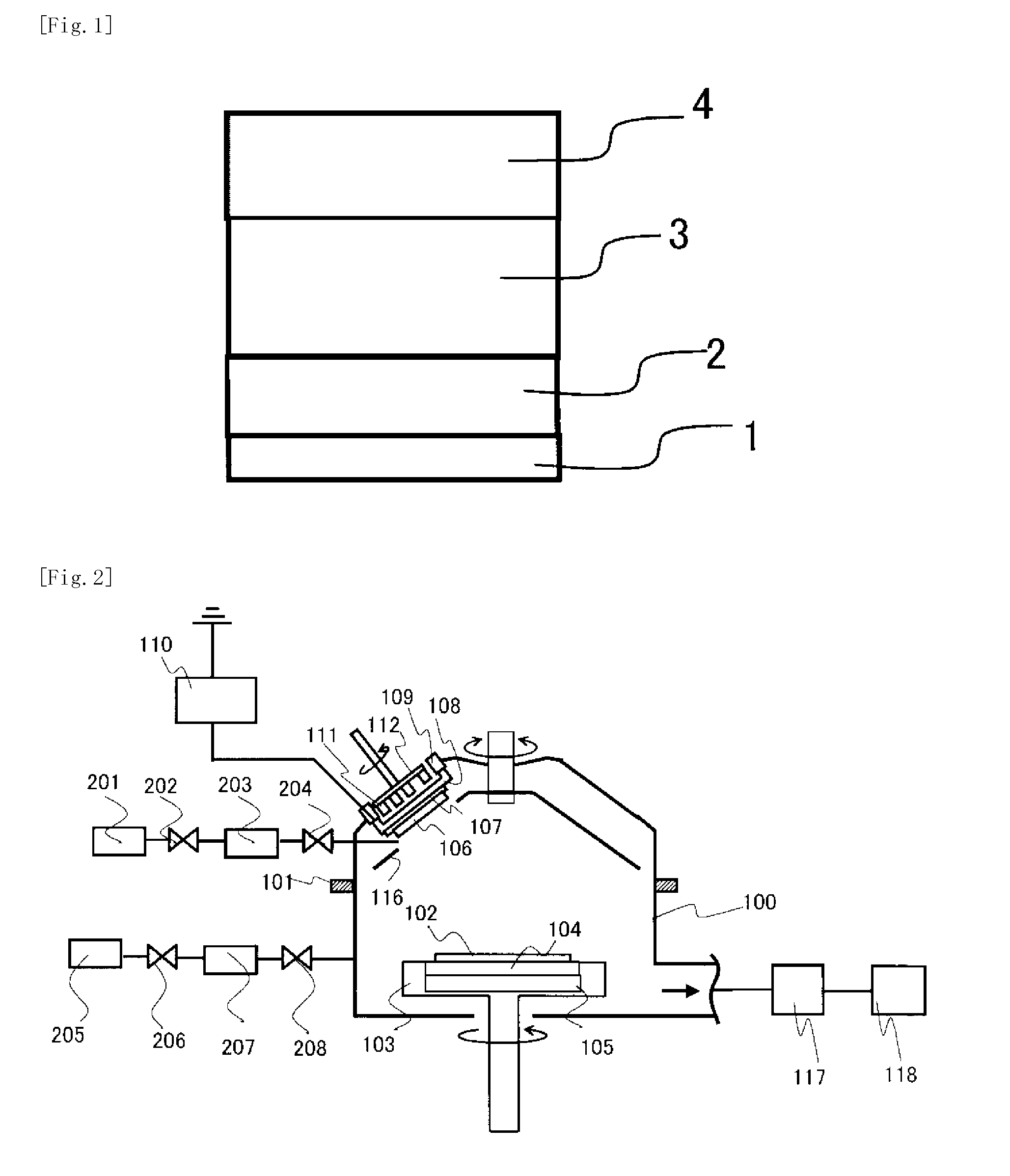
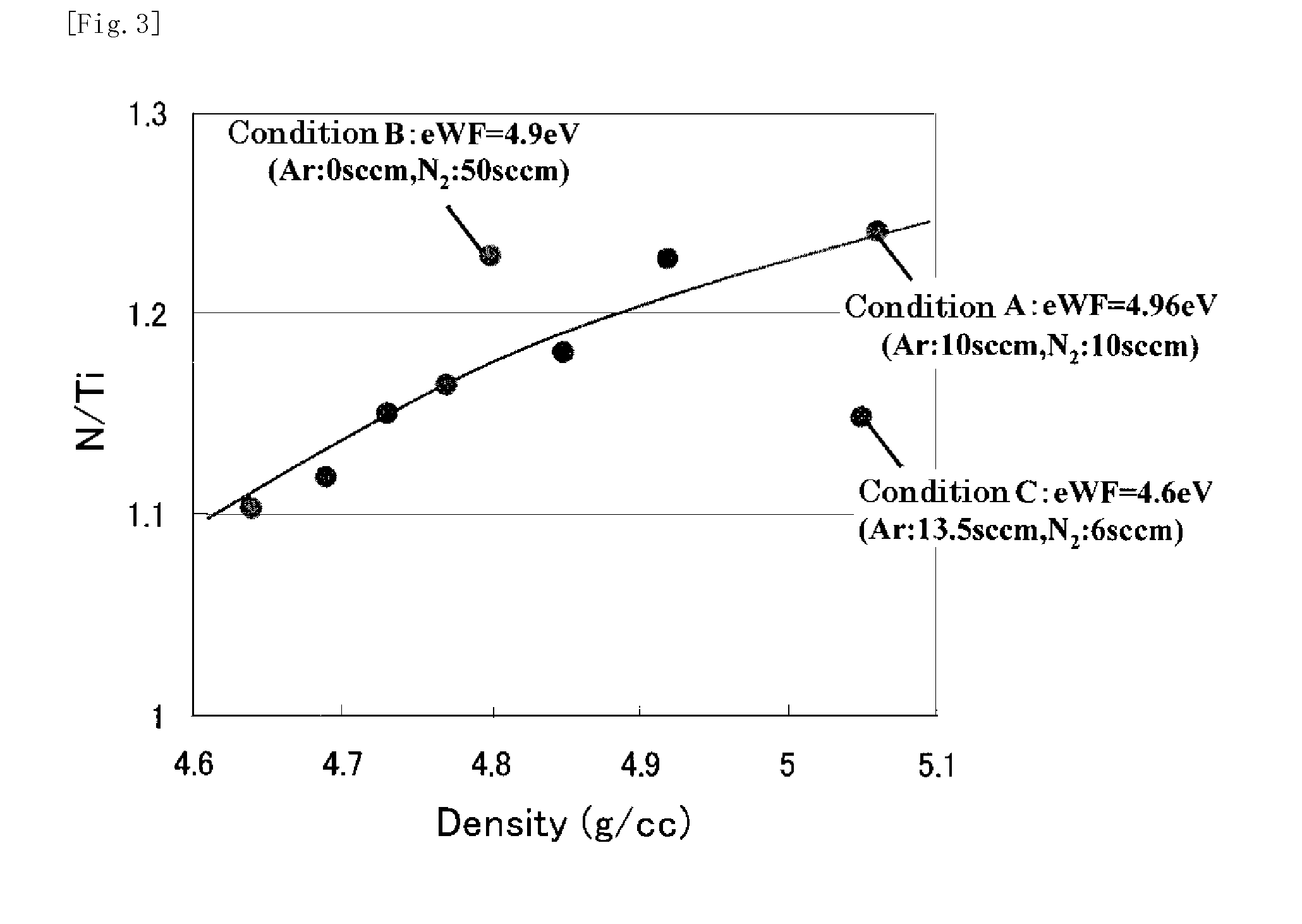
[0090]FIG. 13 shows a schematic cross-section of an element structure having the MIPS type gate electrode according to the example 1. Hf with a film thickness of 0.5 to 0.7 nm is deposited on a silicon substrate 5, having on its surface a silicon oxide film with a film thickness of 1.8 nm, by a sputtering method. Thereafter, an annealing processing at 900° C. for 1 min is applied in an atmosphere with an oxygen partial pressure of 0.1 Pa, and Hf is diffused into the silicon oxide film, whereby a gate insulating film 6 having a stacked structure of the silicon oxide film and an HfSiO film is formed. Thereafter, in the processing apparatus shown in FIG. 2, a titanium nitride film 7 of 2 nm to 5 nm is deposited on the gate insulating film. In the titanium nitride film 7, the blend ratio between an argon gas flow rate and a nitrogen gas flow rate is regulated using a Ti metal target, where...

example 2

[0097]A second example of this invention will be described in detail with reference to the drawings.

[0098]FIGS. 14(a) to 14(c) are views showing processes of a method of manufacturing a semiconductor device shown in FIG. 12 which is the second example of this invention. First, as shown in FIG. 14(a), an element isolation region 302 formed by an STI (Shallow Trench Isolation) technique is provided on the surface of a silicon substrate 301. Subsequently, a silicon thermal oxide film with a film thickness of 1.0 nm is formed on the element-isolated silicon substrate surface by a thermal oxidation method. Thereafter, an HfSiO film is deposited by the same method as in the example 1 to form a gate insulating film 303.

[0099]Next, a titanium nitride film (first metal nitride layer) 304 of 2 nm to 5 nm is deposited on the gate insulating film 303 by the same method as in the example 1. In the titanium nitride film 304, the blend ratio between the argon gas flow rate and the nitrogen gas flo...

example 3

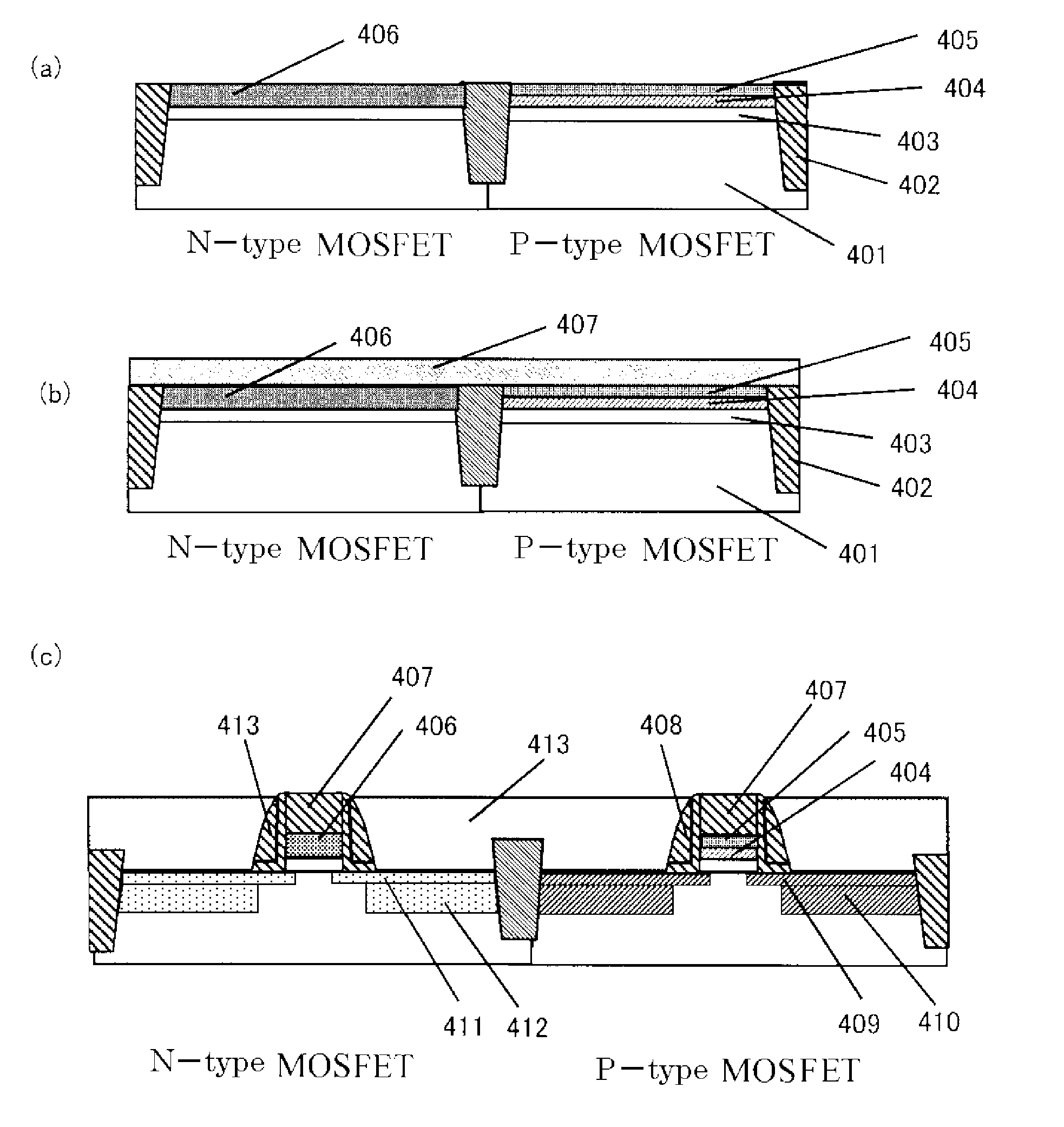
[0107]FIGS. 15(a) to 15(c) are views showing processes of a method of manufacturing a semiconductor device which is the third example of this invention. First, as shown in FIG. 15(a), an element isolation region 402 formed by the STI (Shallow Trench Isolation) technique is provided on the surface of a silicon substrate 401, and an N-type MOSFET region and a P-type MOSFET region are separated from each other. Subsequently, a silicon thermal oxide film with a film thickness of 1.0 nm is formed on the element-isolated silicon substrate surface by a thermal oxidation method. Thereafter, an HfSiO film is deposited by the same method as in the example 1 to form a gate insulating film 903.

[0108]Next, a titanium nitride film (first metal nitride layer) 404 of 2 nm is deposited on the gate insulating film in the P-type MOSFET region by using the processing apparatus shown in FIG. 2. In the titanium nitride film 404, the blend ratio between the argon gas flow rate and the nitrogen gas flow ra...


PUM


Abstract

This invention provides a semiconductor device having a field effect transistor comprising agate electrode comprising a metal nitride layer and a polycrystalline silicon layer, and the gate electrode is excellent in thermal stability and realizes a desired work function.
In the semiconductor device, a gate insulating film 6 on a silicon substrate 5 has a high-permittivity insulating film formed of a metal oxide, a metal silicate, a metal oxide introduced with nitrogen, or a metal silicate introduced with nitrogen,
    • the gate electrode has a first metal nitride layer 7 provided on the gate insulating film 6 and containing Ti and N, a second metal nitride layer 8 containing Ti and N, and a polycrystalline silicon layer 9,
    • in the first metal nitride layer 7, a molar ratio between Ti and N (N/Ti) is not less than 1.1, and a crystalline orientation X1 is 1.1<X1<1.8, and
    • in the second metal nitride layer 8, the molar ratio between Ti and N (N/Ti) is not less than 1.1, and a crystalline orientation X2 is 1.8≦X2.

Description

TECHNICAL FIELD[0001]This invention relates to a semiconductor device, which has a high-permittivity insulating film and a metal gate electrode, a method of manufacturing the semiconductor device, and a manufacturing program, and relates particularly to a technique for improving the performance of an MOSFET (Metal Oxide Semiconductor Field Effect Transistor).BACKGROUND ART[0002]In advanced CMOS (complementary MOS) device development realized miniaturization of a transistor, deterioration of a drive current due to depletion of a polysilicon (poly-Si) electrode and increase in gate current due to thinning of a gate insulating film become problems. Thus, there has been studied a complex technology for preventing the depletion of the electrode by the application of a metal gate, and, at the same time, increasing a physical film thickness by using a high permittivity material in a gate insulating film to thereby reduce gate leak current. For example, a pure metal, a metal nitride, or a s...

Claims


Application Information

Patent Timeline
IPC IPC(8): H01L27/092H01L21/336
CPCH01L21/28088H01L21/823842H01L21/823857H01L29/7833H01L29/517H01L29/6659H01L29/4966H01L29/772
Inventor NAKAGAWA, TAKASHIKITANO, NAOMUMATSUO, KAZUAKIKOSUDA, MOTOMUTATSUMI, TORU
Owner CANON ANELVA CORP
Why Eureka
Try Eureka