SINTERED In-Ga-Zn-O-TYPE OXIDE

a sintered oxide and oxide technology, applied in the direction of diaphragms, metallic material coating processes, electrical devices, etc., can solve the problems of low switching speed, large amount of energy and a large number of steps, and not follow the display of high-speed moving images, etc., to achieve suppressed abnormal discharge or increase in target resistance

Inactive Publication Date: 2012-07-19
IDEMITSU KOSAN CO LTD
View PDF1 Cites 18 Cited by
  • Summary
  • Abstract
  • Description
  • Claims
  • Application Information

AI Technical Summary

Benefits of technology

[0055]Whether the component is the primary component or the sub component is judged by comparing the maximum peak of each component in the X-ray diffraction. Specifically, the height of the maximum peak of each component in the X-ray diffraction is compared, and the component of which the peak height is the highest is defined as the first component and the component of which the peak height is the second highest is defined as the second component. The same is applied to the third and further components.
[0056]In the sputtering target of the invention, the height of the maximum peak in the X-ray diffraction of the compound having a crystal structure represented by β-Ga2O3 is preferably half or less, further preferably a tenth or less, of the height of the maximum peak of the compound having a bixbyite structure represented by In2O3. It is particularly preferred that the maximum peak height of the compound having a crystal structure represented by β-Ga2O3 cannot be confirmed by the X-ray diffraction (the case where the height of the maximum peak of the compound having a crystal structure represented by β-Ga2O3 be a hundredth is defined as the case where it is impossible to confirm by the X-ray diffraction). If the amount of the compound having a crystal structure represented by β-Ga2O3 is small, an increase in target resistance or generation of abnormal discharge can be suppressed.
[0057]Similarly, the height of the maximum peak in the X-ray diffraction of the compound having a homologous crystal structure represented by In2Ga2ZnO7 or InGaZnO4 is preferably half or less, further preferably a tenth or less, of the height of the maximum peak of the compound having a crystal structure represented by In2O3. It is particularly preferred that the maximum peak height of the compound having a homologous crystal structure represented by In2Ga2ZnO7 or InGaZnO4 cannot be confirmed by the X-ray diffraction. For example, if the maximum peak height of the compound having...

Problems solved by technology

However, since the switching speed thereof is low as compared with a crystalline thin film, when used as a switching device for driving a display, it may not follow the display of a high-speed moving image.
On the other hand, although a crystalline silicon-based thin film has a high degree of mobility, it has a problem that a large amount of energy and a large number of steps are required for the production and that an increase in area is difficult.
For example, when crystallizing a silicon-based thin film, laser annealing which requires a high temperature of 800° C. or higher or expensive equipment is required.
Further, as for a crystalline silicon-based thin film, since the device configuration of a TFT is normally restricted to a top-gate structure, a decrease in cost such...

Method used


Image

  • SINTERED In-Ga-Zn-O-TYPE OXIDE
  • SINTERED In-Ga-Zn-O-TYPE OXIDE
  • SINTERED In-Ga-Zn-O-TYPE OXIDE

Examples


example 1

Preparation of an Oxide Sintered Body

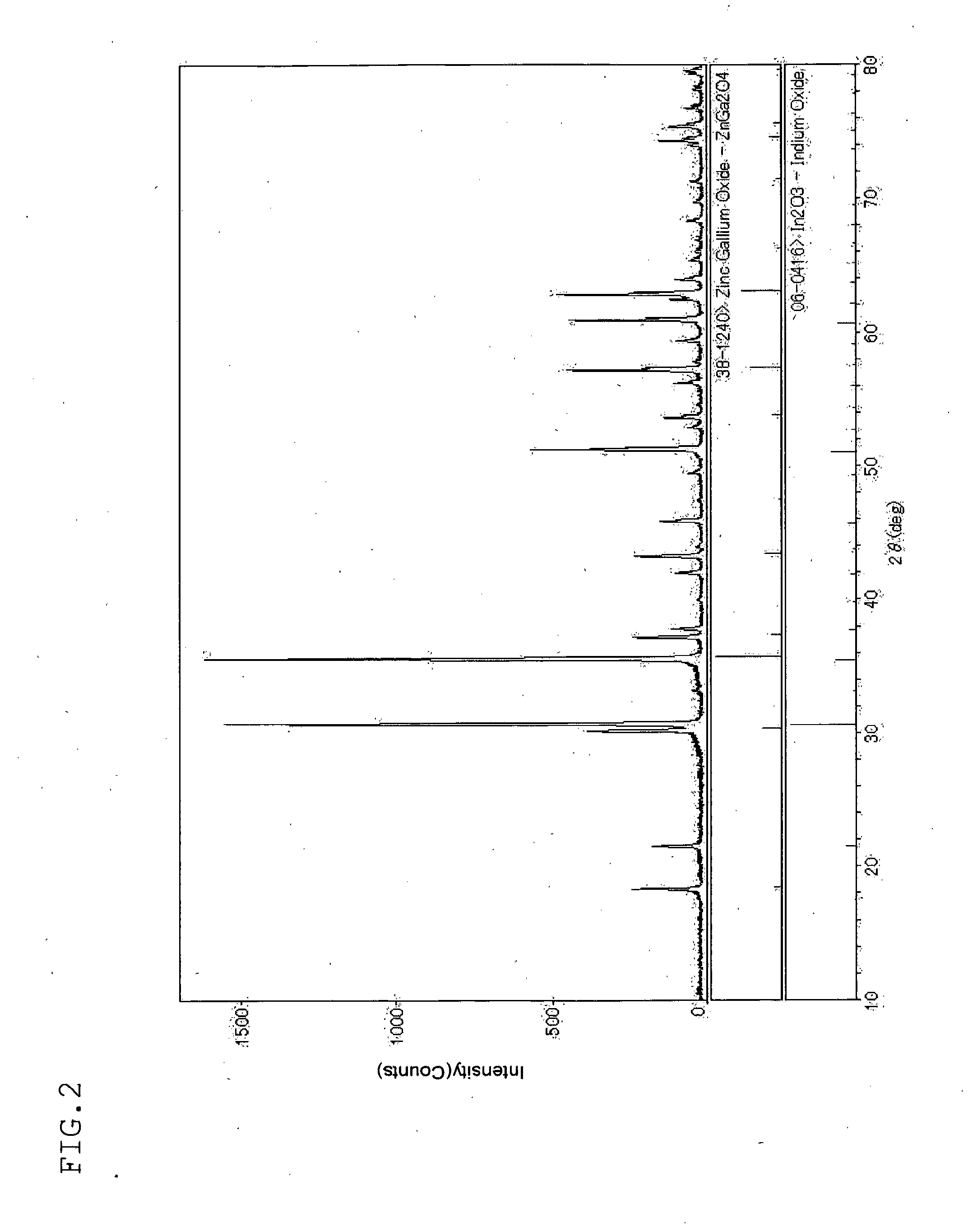
[0145]As the raw material powder, powder of In2O3 (specific surface area: 11 m2 / g, purity: 99.99%), Ga2O3 (specific surface area: 11 m2 / g, purity: 99.99%) and ZnO (specific surface area: 9 m2 / g, purity: 99.99%) were used. The raw material was mixed such that the atomic composition ratio shown in Table 1 was attained. The resulting mixture was mixed by means of a super mixer for 4 minutes. Mixture was conducted in the air with a revolution of 3000 rpm.

[0146]The resulting mixture powder was retained in an electric furnace in an atmosphere at 1000° C. for 5 hours to conduct pre-firing. The resulting pre-fired powder was put into an attritor together with zirconia beads, and the resultant was finely pulverized at a revolution of 300 rpm for 3 hours. After the pulverization, the raw material powder had an average particle size (D50) of 0.55 μm.

[0147]To the thus finely pulverized raw material powder, water was added such that slurry having a solid matt...

example 3

(A) Preparation of an Oxide Sintered Body

[0169]In2O3 powder having a specific surface area of 15 m2 / g and purity of 99.99%, Ga2O3 powder having a specific surface are of 14 m2 / g and purity of 99.99% and ZnO powder having a specific surface area of 4 m2 / g and purity of 99.99% were compounded, and the resultant was mixed and pulverized by means of a ball mil until the grain size of each raw material powder became 1 μm or less. The thus obtained slurry was taken out, and rapidly dried and granulated by means of a spray drier at a slurry supply speed of 140 ml / min, a hot air temperature of 140° C. and a hot air amount of 8 Nm3 / min. The granulated product was shaped at a pressure of 3 tons / cm2 by cold isostatic pressing, thereby to obtain a shaped product.

[0170]Subsequently, this shaped product was sintered. During the sintering, the temperature was elevated at a rate of 0.5° C. / min in the air until it reached 600° C., and thereafter, in the range of 600° C. to 800° C., the temperature w...


PUM

PropertyMeasurementUnit
Temperatureaaaaaaaaaa
Fractionaaaaaaaaaa
Timeaaaaaaaaaa

Abstract

An oxide sintered body including In (indium element), Ga (gallium element) and Zn (zinc element), having a total content of In, Ga and Zn relative to total elements except for an oxygen element of 95 at % or more, and including a compound having a bixbyite structure represented by In2O3 and a compound having a spinel structure represented by ZnGa2O4.

Description

TECHNICAL FIELD[0001]The invention relates to an oxide sintered body. In particular, the invention relates to an oxide sintered body suited for the formation of an amorphous oxide film by sputtering.BACKGROUND ART[0002]A field effect transistor such as a thin film transistor (TFT) is widely used as a unit electronic device of a semiconductor memory integrated circuit, a high-frequency signal amplification device and a liquid crystal driving device. A field effect transistor is an electronic device which is most widely put into practice currently. Of these, with a significant development of a display in recent years, in various displays such as a liquid crystal display (LCD), an electroluminescence display (EL) and a field emission display (FED), a TFT is frequently used as a switching device for driving a display by applying a driving voltage to a display device.[0003]As the material for the semiconductor layer (channel layer) which is the main component of the field effect transist...

Claims


Application Information

Patent Timeline
IPC IPC(8): H01L21/20C23C14/08C04B35/64C23C14/34
CPCC04B35/01H01L29/66969C04B35/62695C04B2235/3232C04B2235/3244C04B2235/3256C04B2235/3284C04B2235/3286C04B2235/3287C04B2235/3293C04B2235/3418C04B2235/5409C04B2235/5445C04B2235/604C04B2235/656C04B2235/6562C04B2235/6567C04B2235/6585C04B2235/76C04B2235/763C04B2235/77C04B2235/80C04B2235/96C23C14/08C23C14/3414H01L21/02554H01L21/02565H01L21/02631H01L29/7869C04B35/453C04B35/00C23C14/34H01L21/34
Inventor YANO, KOKIKAWASHIMA, HIROKAZUITOSE, MASAYUKIINOUE, KAUZYOSHI
Owner IDEMITSU KOSAN CO LTD
Why Eureka
Try Eureka