Electrode and method for manufacturing the same

a technology of electric devices and electrodes, applied in the manufacture of electric discharge tubes/lamps, inorganic insulators, instruments, etc., can solve the problems of increasing capital investment, requiring a sharp rise in material costs, and copper cannot be sintered in air, so as to achieve a reduction in the cost of production

Inactive Publication Date: 2012-10-11
EI DU PONT DE NEMOURS & CO
View PDF0 Cites 2 Cited by
  • Summary
  • Abstract
  • Description
  • Claims
  • Application Information

AI Technical Summary

Benefits of technology

[0011]An electrode with the above characteristics can be achieved by configuring a paste comprising boron powder as the top layer of an electrode containing copper powder, another easily oxidizable metal, or an alloy thereof as the conductive component.
[0025]The present invention enables the formation of a low-resistance pattern by air firing using an inexpensive conductive component. The present invention will contribute to a decrease in the cost of producing an electrode for an electronic device.

Problems solved by technology

Using precious metals, however, invites a sharp rise in material costs because precious metals are expensive.
However, copper cannot be sintered in air because it oxidizes easily, and this increases capital investment because firing under a nitrogen atmosphere and the like is required.

Method used


Image

  • Electrode and method for manufacturing the same
  • Electrode and method for manufacturing the same
  • Electrode and method for manufacturing the same

Examples


example 1

1. Preparation of Organic Components

[0105]Texanol (2,2,4-trimethyl-1,3-pentanediol monoisobutyrate) as the solvent and acrylic polymer binder having a molecular weight of 6,000 to 7,000 as the organic binder were mixed, and the mixture was heated to 100° C. while stirring. The mixture was heated and stirred until all of the organic binder had dissolved. The resulting solution was cooled to 75° C. EDAB (ethyl 4-dimethyl aminobenzoate), DETX (diethylthioxanthone), and Irgacure 907 by Chiba Specialty Chemicals were added as photo polymerization initiator, and TAOBN (1,4,4-trimethyl-2,3-diazabicyclo[3.2.2]-non-2-ene-N,N-dixoide) was added as a stabilizer. The mixture was stirred at 75° C. until all the solids had dissolved. The solution was filtered through a 40 micron filter and cooled.

2. Preparation of Paste

2-1: Preparation of Paste 1 (Cu)

[0106]A photopolymerization monomer consisting of 2.62 wt % TMPEOTA (trimethylolpropane ethoxytriacrylate), 2.62 wt % Laromer® LR8967 (polyethyl acr...

examples 2-5

Comparative Examples 7-8

[0131]Pattern forming was attempted using Paste 2 (B), Paste 3 (Cu), and Paste 4 (Ni) shown in Table 1.

TABLE 4ComparativeComparativeEx. 2Ex. 3Ex. 7Ex. 8Ex. 4Ex. 5Top LayerPaste 2 (B)Paste 2 (B)NoneNonePaste 2 (B)Paste 2 (B)Bottom LayerPaste 3 (Cu)Paste 4 (Ni)Paste 3 (Cu)Paste 4 (Ni)Paste 3 (Cu)Paste 4 (Ni)Thickness of dried film11.7511.45.259.35(um)Surface resistance Ohm0.1954.5859115004.00E+07——Volume resistivity Ohm · cm1.28E−056.98E−04N / MN / M2.21E−055.31E−04Photo patterningOKOK——OKOK

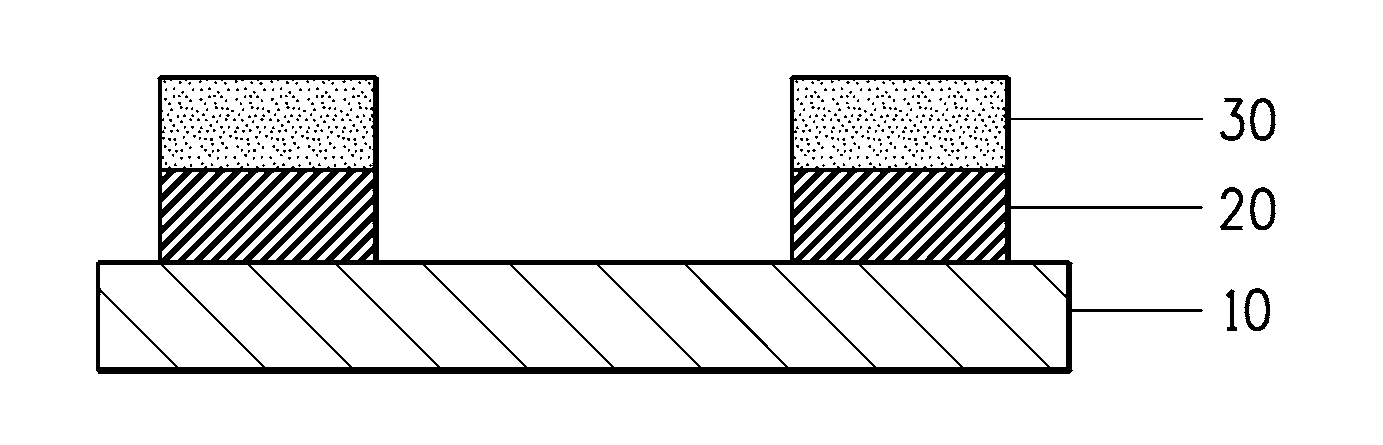
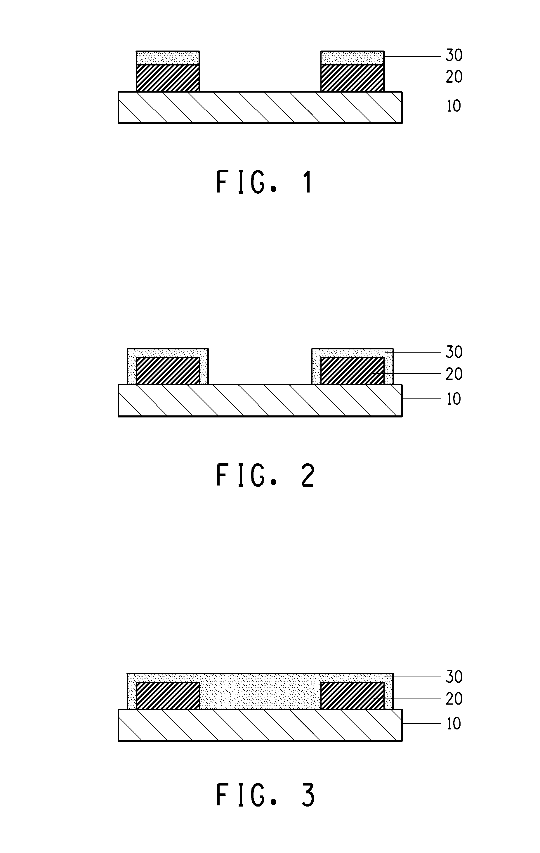
[0132]For Examples 2 and 3 in Table 4, the bottom layer was configured by coating and drying a paste containing copper or nickel conductive powder, respectively, and after a paste containing boron was coated as the top layer, the bilayer dried films were exposed and developed. In this case the cross-sectional structure of the formed pattern is the one illustrated in FIG. 1. In Example 2 the surface resistance was 0.195Ω and the volume resistivity was 1.28×10⁻⁵ Ω·cm, and in Examp...

examples 6-8

Comparative Examples 9-11

[0134]Pattern forming was attempted using Paste 5 (Cu+Sn), Paste 6 (Bi+Sn), Paste 7 (Cu+solder), and Paste 8 (B) shown in Table 5.

TABLE 5Paste 5Paste 6Paste 7Paste 8(Cu + Sn)(Bi + Sn)(Cu + Solder)(B)Medium (binder, initiator, solvent)18.0013.1713.1742.76Antifoamer (silicone oil)0.38Dispersant (Soya lecithin)0.580.610.61Malonic acid (viscosity stabilizer)1.83Solvent (Texanol)0.450.480.485.24Monomer28.76(TMPEOTA:Laromer ® LR8967:Sartomer ®SR399 = 1:1:3)Glass frit (Nippon Yamamura Glass)2.903.073.070.26Boron (H. C. Starck, Grade I)20.77Braze Tec CTF600, Cu 76, Sn 15, Ni 4,78.07P 5 Alloy in a form of thermoplasticpaste, Tm 590-600 CMitsui Kinzoku, Sn42% / Bi58% alloy,82.685um powderMitsui Kinzoku, SAC305,41.34Sn96.5% / Ag 3% Cu 0.5%, Pb-freesolder alloy, 5um powderCopper (DOWA electronics, D50 = 1.0 μm)41.34Total100.00100.00100.00100.00

[0135]Resistance was measured in the fired films prepared by configuring a conductive layer using pastes containing the various meta...


PUM

PropertyMeasurementUnit
particle sizeaaaaaaaaaa
diameteraaaaaaaaaa
diameteraaaaaaaaaa

Abstract

Disclosed is an electrode, including a conductive layer containing a conductive component selected from the group consisting of copper, nickel, iron, cobalt, titanium, lead, aluminum, tin, and alloys comprising one of these metals as the principal ingredient thereof, and an oxidation protection layer containing boron oxide, said oxidation protection layer covering the top surface of the conductive layer, or covering both the top surface and the sides of the conductive layer, or covering all locations where the conductive layer has been formed; the electrode being formed by air firing the conductive layer and the oxidation protection layer simultaneously.

Description

[0001]This application is a continuation of Ser. No. 12 / 576,328, filed on Oct. 9, 2009.BACKGROUND OF THE INVENTION[0002]1. Field of the Invention[0003]The present invention relates to an electrode of an electric device, and more particularly to improvements in the structure of the electrode.[0004]2. Technical Background[0005]Methods wherein a conductive paste is used as the raw material of an electrode are widely known. The conductive paste generally comprises a conductive component, glass frit, organic binder, and solvent. Photosensitive paste, which enables fine pattern formation, is also widely used, and the composition of the photosensitive paste generally includes monomer and photoinitiator in addition to the aforementioned components.[0006]Non-photosensitive paste is coated in a predetermined pattern by screen printing or another method, and an electrode consisting of glass with a conductive component and binder is formed therefrom by drying and firing. Photosensitive paste (n...

Claims


Application Information

Patent Timeline
Patent Type & Authority Applications(United States)
IPC IPC(8): H01B3/10B05D3/02B05D5/12H05K1/03G03F7/20
CPCG03F7/0047G03F7/027H01J2211/40H01J9/02H01J2211/225H01B1/22H05K1/092H05K3/282H05K2203/1126
Inventor KUROKI, MASAKATSU
Owner EI DU PONT DE NEMOURS & CO
Why Eureka
Try Eureka