Method for manufacturing graphene, transparent electrode and active layer comprising the same, and display, electronic device, optoelectronic device, battery, solar cell, and dye-sensitized solar cell including the electrode and the active layer

a transparent electrode and active layer technology, applied in the field of manufacturing graphene, can solve the problems of increasing the cost of ito, and reducing the service life of the transparent electrode using ito, etc., to achieve excellent chemical, optical and electrical characteristics, easy patterned, excellent physical and electrical characteristics

Inactive Publication Date: 2012-12-27
UNIST ACAD IND RES CORP
View PDF9 Cites 44 Cited by
  • Summary
  • Abstract
  • Description
  • Claims
  • Application Information

AI Technical Summary

Benefits of technology

[0051]In addition, the graphene may be easily patterned with desired geometries at particular locations by using a pre-patterned metal thin film via a self-assembly or a conventional patterning method.
[0052]The graphene may be used to fabricate a display, an optoel

Problems solved by technology

However, the cost of ITO increases as more indium is consumed and indium becomes scarcer.
Further, a transparent electrode using ITO is known to have chemical and electrical characteristic defects.
The use of such a low mobility layer in electric devices for an excellent characteristic may be di

Method used


Image

  • Method for manufacturing graphene, transparent electrode and active layer comprising the same, and display, electronic device, optoelectronic device, battery, solar cell, and dye-sensitized solar cell including the electrode and the active layer
  • Method for manufacturing graphene, transparent electrode and active layer comprising the same, and display, electronic device, optoelectronic device, battery, solar cell, and dye-sensitized solar cell including the electrode and the active layer
  • Method for manufacturing graphene, transparent electrode and active layer comprising the same, and display, electronic device, optoelectronic device, battery, solar cell, and dye-sensitized solar cell including the electrode and the active layer

Examples


example

Preparation of Graphene

Example 1

Direct Growth of Graphene on a SiO2 / Si Substrate

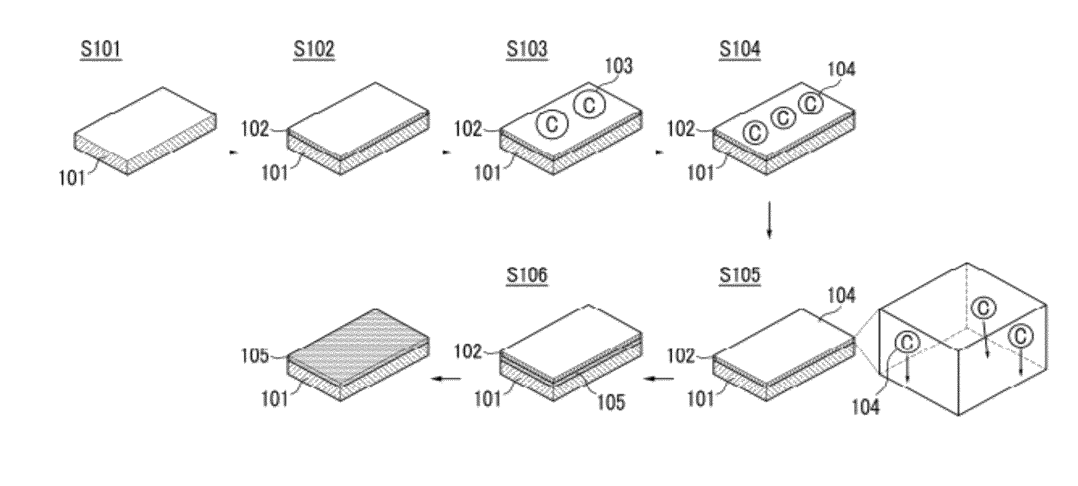
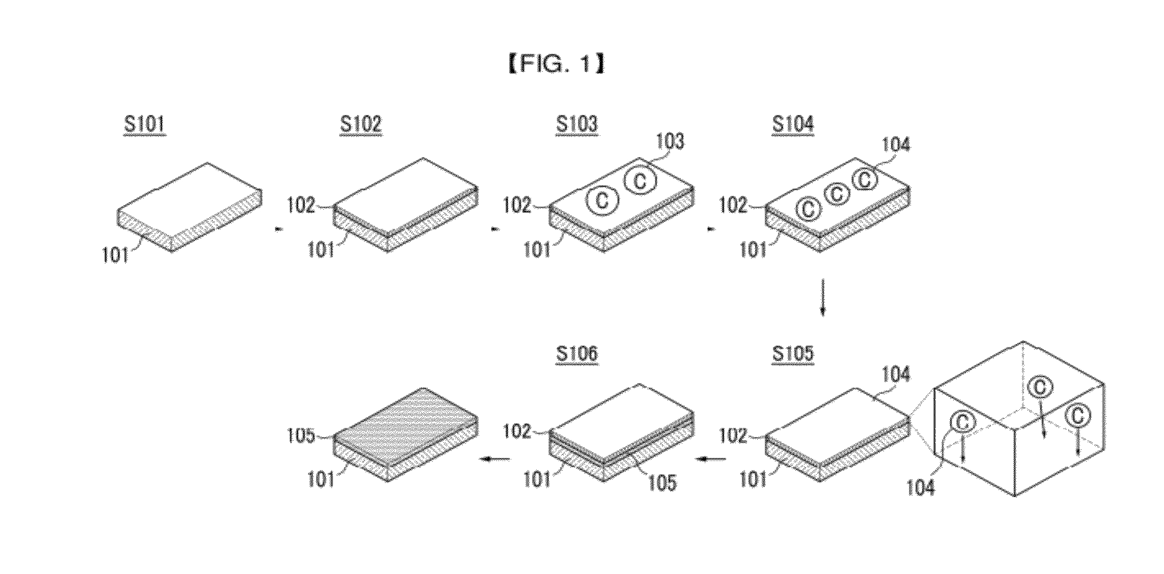
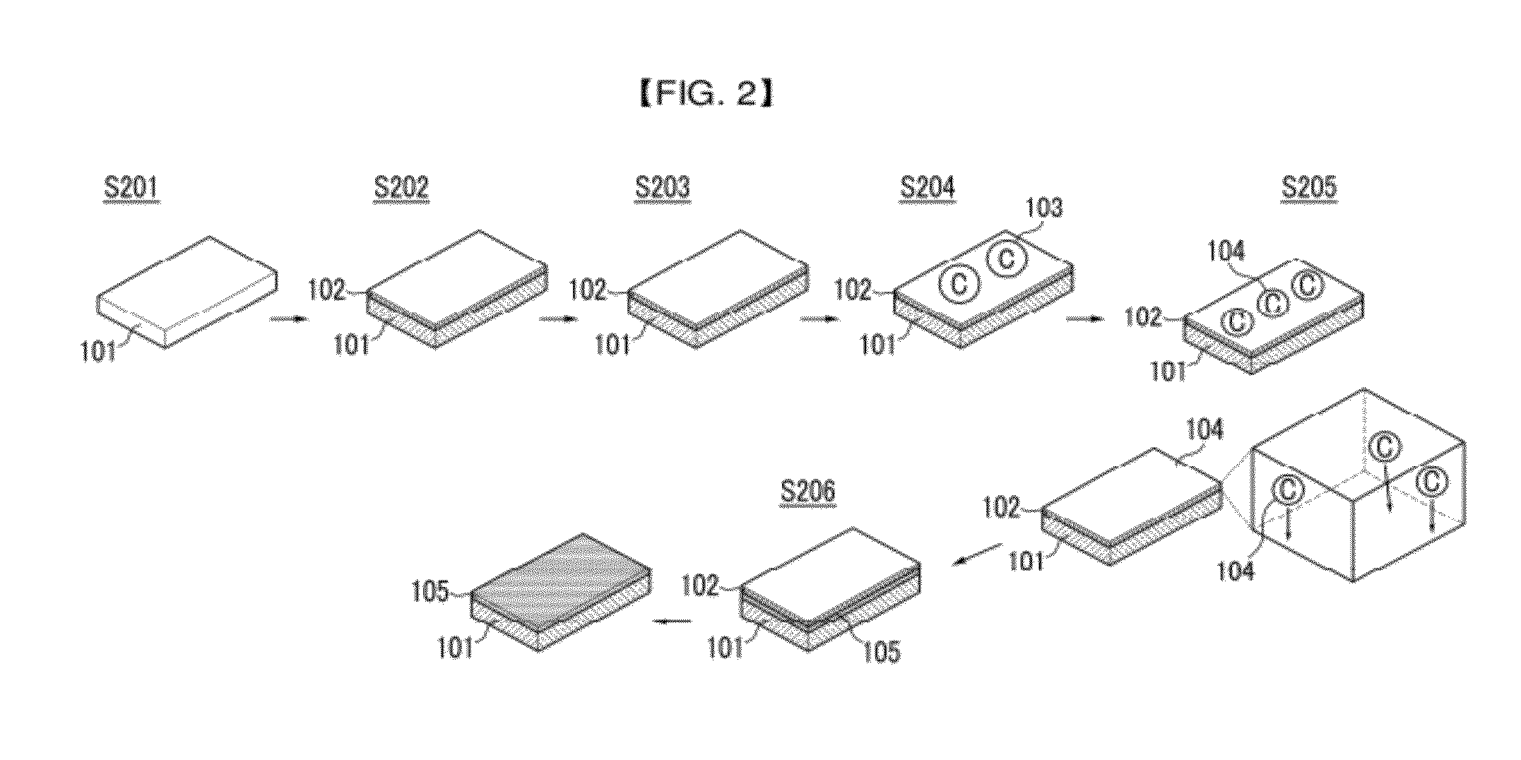
[0175]A liquid carbon source material according to one embodiment of the present invention was used to directly grow graphene on a SiO2 / Si substrate. The SiO2 was a 300 nm-thick layer and was deposited on a Si substrate in a conventional thermal growth method.

[0176]The surface of the SiO2 / Si substrate was cleaned. Then, a 100 nm-thick nickel thin film was deposited on the SiO2 / Si substrate using an electron beam evaporator. The SiO2 / Si substrate was maintained at 400° C. during the nickel deposition.

[0177]FIG. 3 provides a SEM image of the deposited nickel thin film.

[0178]The SEM image shows that the nickel thin film was polycrystalline. It had grains with an average size of about 100 nm.

[0179]The nickel thin film was heat-treated to improve the orientation and to increase the average grain size. The heat treatment was performed in a high-vacuum chamber. The chamber was under a hydrogen atmosphere using ...

example 2

[0186]Graphene was formed according to the same method as Example 1, except that heating temperature was 160° C. after putting a carbon source material onto a nickel thin film.

[0187]FIG. 6 provides SEM images of the graphene according to Example 2. As shown in FIG. 6, the graphene according to Example 2 had a large grain with average size ranging from several μm to tens of μm. The SEM images show clear brightness contrast depending on the thickness. The lightest image indicates a monolayer graphene C, the light image indicates a bilayer graphene B, and the darkest image indicates multi-layered graphene A.

[0188]In addition, as shown in FIG. 6, the graphene according to Example 2 was formed at a low temperature and thus had no creases due to the difference in thermal expansion coefficients between the graphene and an underlying substrate. In general, the crease might deteriorate physical properties of the graphene.

example 3

[0189]Graphene was formed according to the same method as Example 1, except that heating temperature and time were 60° C. and 10 minutes, respectively, after putting a carbon source material onto a nickel thin film.


PUM

PropertyMeasurementUnit
Temperatureaaaaaaaaaa

Abstract

Disclosed is a method of manufacturing graphene, a transparent electrode and an active layer including the graphene, and a display, an electronic device, an optoelectronic device, a solar cell, and a dye-sensitized solar cell including the transparent electrode and the active layer. The method of manufacturing graphene includes: (a) preparing a subject substrate; (b) forming a metal thin film on the subject substrate and heat-treating the metal thin film to increase the grain size of the metal thin film; (c) supplying a carbon source material on the metal thin film; (d) heating the supplied carbon source material, the subject substrate, and the metal thin film; (e) diffusing carbon atoms generated from the heated carbon source material due to thermal decomposition into the metal thin film; and (f) forming graphene on the subject substrate by the carbon atoms diffused through the metal thin film.

Description

CROSS-REFERENCE TO RELATED APPLICATION[0001]This is a continuation of international application no. PCT / KR2011 / 001092 filed on Feb. 18, 2011, which claims priority to and the benefit of Korean Patent Application No. 10-2010-0020990 filed in the Korean Intellectual Property Office on Mar. 9, 2010 and Korean Patent Application No. 10-2010-0126995 filed in the Korean Intellectual Property Office on Dec. 13, 2010, the entire contents of which are incorporated herein by reference.BACKGROUND OF THE INVENTION[0002](a) Field of the Invention[0003]The present invention relates to a method of manufacturing graphene, a transparent electrode and an active layer including the same, and a display, an electronic device, an optoelectronic device, a battery, a solar cell, and a dye-sensitized solar cell including the electrode and / or the active layer.[0004](b) Description of the Related Art[0005]In general, since various devices such as a display, a light emitting diode, a solar cell, and the like t...

Claims


Application Information

Patent Timeline
IPC IPC(8): B05D5/12B32B9/04C01B31/00B82Y30/00B82Y40/00
CPCB82Y30/00B82Y40/00C01B31/0446H01L31/022466H01L31/1884H01M4/663Y02E10/542H01B1/04G02F1/15G02F1/155H01M4/587H01L51/442C01B32/184Y02E10/549Y02P70/50Y02E60/10H10K30/82C01B32/186
Inventor KWON, SOON-YONGPARK, KIBOGYOON, EUIJOONKWAK, JIN-SUNG
Owner UNIST ACAD IND RES CORP
Why Eureka
Try Eureka