Chip for protein detection, method for manufacturing the same, and method for detecting protein by using the same

Inactive Publication Date: 2013-02-28
NAT CHENG KUNG UNIV
View PDF1 Cites 8 Cited by
  • Summary
  • Abstract
  • Description
  • Claims
  • Application Information

AI Technical Summary

Benefits of technology

[0024]In addition, the ratio of the fluoro-containing compound and the carboxyl-containing compound in the mixture solution depends upon the carbon number of the long chain fluoro-alkyl group. After the substrate is coated with the mixture solution, a fluorinated layer is formed on the covalent modification layer, especially the intermediate layer. The activated carboxyl groups fr

Problems solved by technology

When these substrates are applied to protein microarrays, the problems of low protein binding density, spread of the spotted material, and low signal-to-noise ratio may occur.
However, since small sample volumes (nanoliter) are applied to the hydrophilic plain glass surface, the sample may be easily evaporated.
However, such hydrophilic surface formed by molecules like polylysine would not allow forming microliter droplets, which will spread out on t

Method used


Image

  • Chip for protein detection, method for manufacturing the same, and method for detecting protein by using the same
  • Chip for protein detection, method for manufacturing the same, and method for detecting protein by using the same
  • Chip for protein detection, method for manufacturing the same, and method for detecting protein by using the same

Examples


embodiment 1

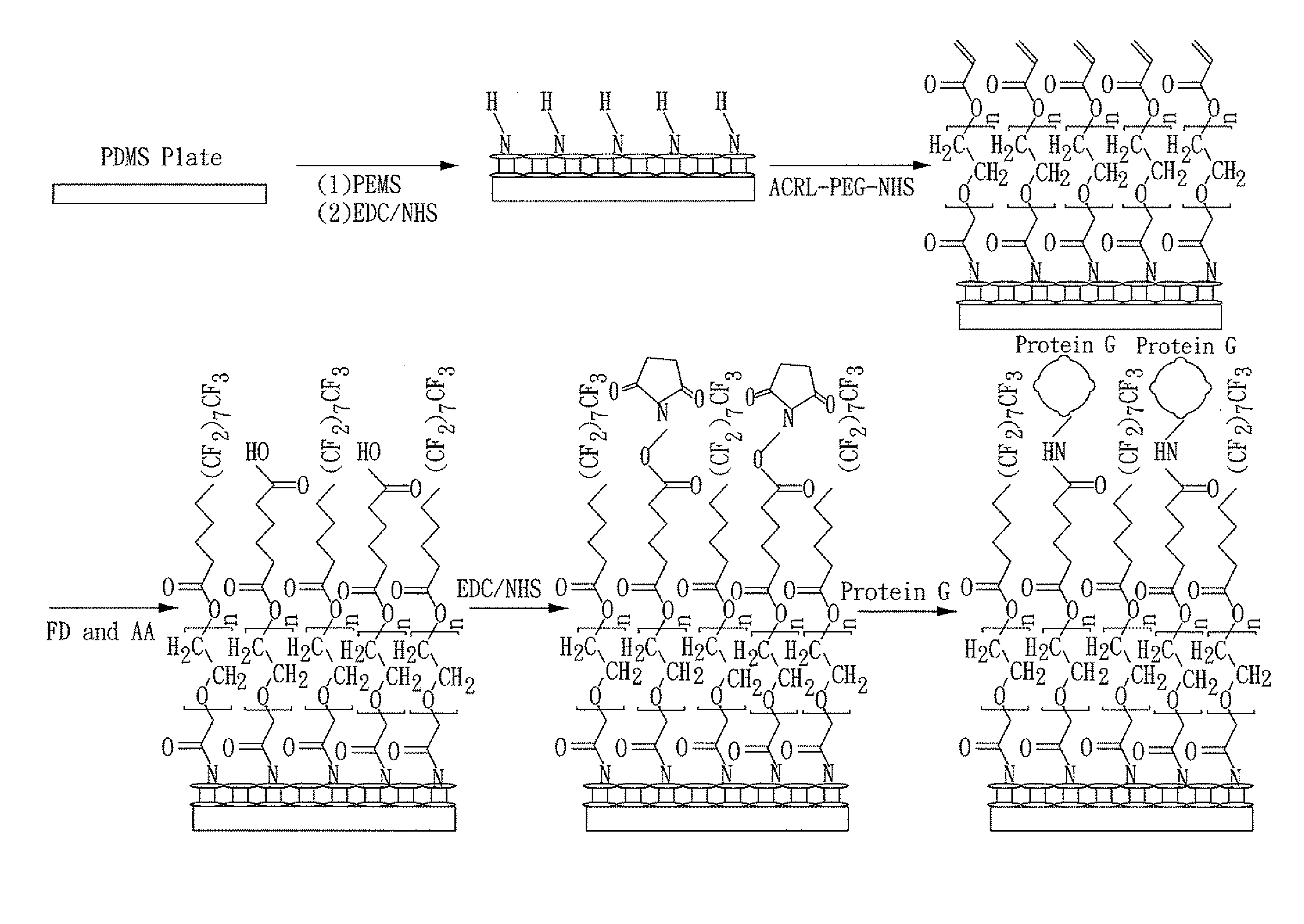
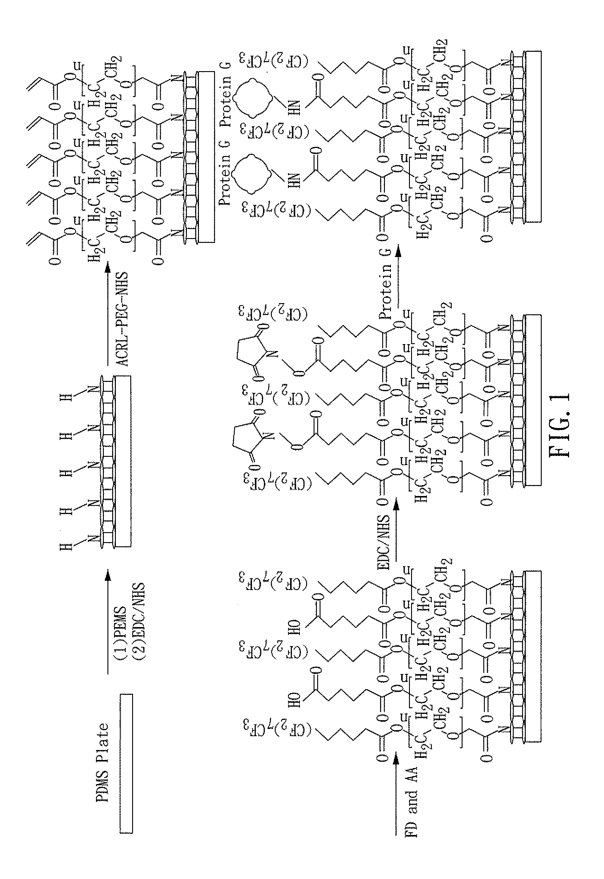
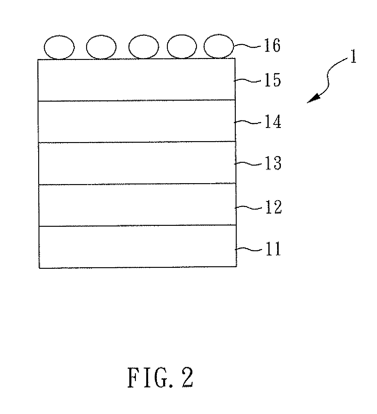
A Chip for Protein Detection with a PDMS Substrate Preparation of a Chip for Protein Detection

[0038]The process for forming the chip for protein detection of the present embodiment is shown in FIG. 1.

[0039]To form the PDMS prepolymer, the PDMS oligomer was mixed with a curing agent at a weight ratio of 10:1, and the resulting mixture was degassed in a vacuum for 30 min. The degassed PDMS mixture was poured on the stainless steel plate for matrix assisted laser desorption / ionization instrument (MALDI, Waters) and then cured at 70° C. for four hours. Once peeled from the stainless steel plate, the resulting 12×8 array pattern (2.5 mm id for each spot in a space of 5 cm width×4 cm length) of the PDMS substrate was used as the grid for solution printing.

[0040]The bare substrate was then modified with polyelectrolyte multilayers (PEMS). The process for modifying the bare substrate is briefly described as follow. First, the bare PDMS substrates were activated by an oxygen plasma, subseque...

embodiment 2

A Chip for Protein Detection with a Glass Substrate Preparation of a Chip for Protein Detection

[0061]The process for forming the chip for protein detection of the present embodiment is similar to that of Embodiment 1, except that PDMS substrate is substituted with a glass substrate.

[0062]First, the bare glass substrate was activated by an oxygen plasma, and subsequently coated with 3-Aminopropyl triethoxysilane (APTES) to form a covalent modification layer on the surface of the glass substrate. Then, ACRL-PEG-NHS (1000 μg / mL in PBS, pH 7.4) was added to react with the exposed amine group of APTES molecules in the covalent modification layer. Therefore, an intermediate layer was formed on the glass substrate.

[0063]The same process for forming the fluorinated layer described in Embodiment 1 was performed in the present embodiment to form a fluorinated layer on the glass substrate. Then, the same process for coating the protein G described in Embodiment 1 was also performed in the pres...


PUM


Abstract

A chip for protein detection, a method for manufacturing the same, and a method for detecting protein by using the chip are provided in the present invention. The chip for protein detection of the present invention comprises: a substrate; a covalent modification layer disposed on the substrate; a fluorinated layer disposed on the covalent modification layer, wherein the fluorinated layer comprises fluorinated functional groups and bio-molecular binding groups; and antibody-binding molecules connecting to the bio-molecular binding groups.

Description

BACKGROUND OF THE INVENTION[0001]1. Field of the Invention[0002]The present invention relates to a chip for protein detection, a method for manufacturing the same, and a method for detecting protein by using the chip. More specifically, the present invention relates to a chip for protein detection with resistance against nonspecific bonding, and a method for manufacturing the same. In addition, the present invention also relates to a method for detecting protein by using the aforementioned chip for protein detection, to detect low-content target molecules.[0003]2. Description of Related Art[0004]Array-based technologies are excellent analytical platforms for a broad range of applications including medical testing, environmental testing, food testing, new drug development, basic research, military defense, and chemical synthesis. Various substrates, including hard materials like glass and soft materials like nitrocellulose or polydimethylsiloxane (PDMS), have been widely used for the...

Claims


Application Information

Patent Timeline
IPC IPC(8): C40B30/04G01N1/31C40B60/12
CPCG01N33/54353G01N33/68G01N33/54393
Inventor CHEN, SHU-HUICHEN, HUANG-HAN
Owner NAT CHENG KUNG UNIV
Why Eureka
Try Eureka