Method and composition for removing resist, etch residue, and copper oxide from substrates having copper, metal hardmask and low-k dielectric material

Active Publication Date: 2013-06-20
EKC TECH
View PDF7 Cites 38 Cited by
  • Summary
  • Abstract
  • Description
  • Claims
  • Application Information

AI Technical Summary

Benefits of technology

[0014]The compositions and method according to the inventive concepts described herein are uniquely capable of selectively etching TiN, TiNxOy or W, are compatible with Cu and low-k dielectric materials, and can also simultaneously remove copper oxides, polymeric materials and etch residues from the substrate being treated. A composition formulated according to the invention and exhibiting an inherently high etch rate for TiN, TiNxOy or W enables processing at low temperature, e.g., temperatures less than 65° C. A relatively low temperature process exhibits a reduced oxidizer decomposition rate, which, in turn, extends the useful composition bath life. Additionally, compositions according to the invention which exhibit high TiN, TiNxOy or

Problems solved by technology

As the technology nodes advance to 45 nm and smaller, the decreasing size of semiconductor devices makes achieving critical profile control of vias and trenches more challenging.
Fabrication of advanced generation devices that require copper conductors and low-k dielectric materials (typically carbon-silica or porous silica materials), give rise to the problem that both

Method used


Image

  • Method and composition for removing resist, etch residue, and copper oxide from substrates having copper, metal hardmask and low-k dielectric material
  • Method and composition for removing resist, etch residue, and copper oxide from substrates having copper, metal hardmask and low-k dielectric material
  • Method and composition for removing resist, etch residue, and copper oxide from substrates having copper, metal hardmask and low-k dielectric material

Examples


examples

[0045]Compositions according to the invention are now explained in detail by reference to the inventive concepts and comparative examples which follow, but the present invention is not limited by these examples.

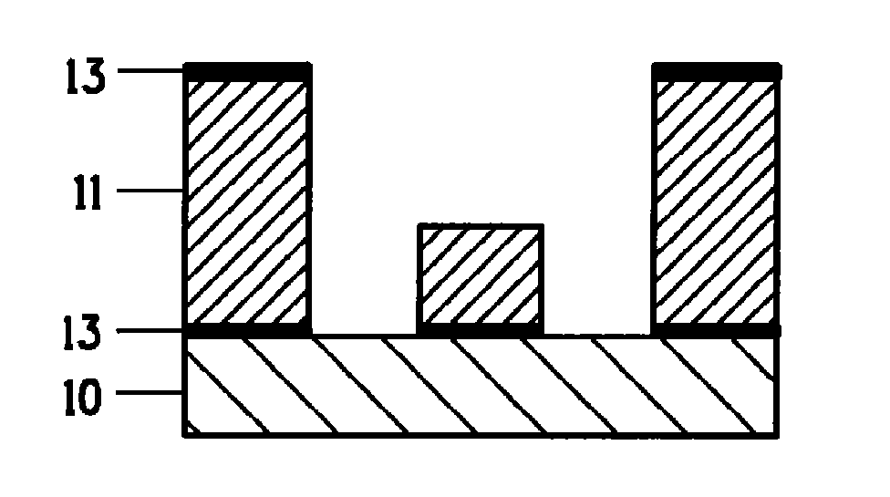
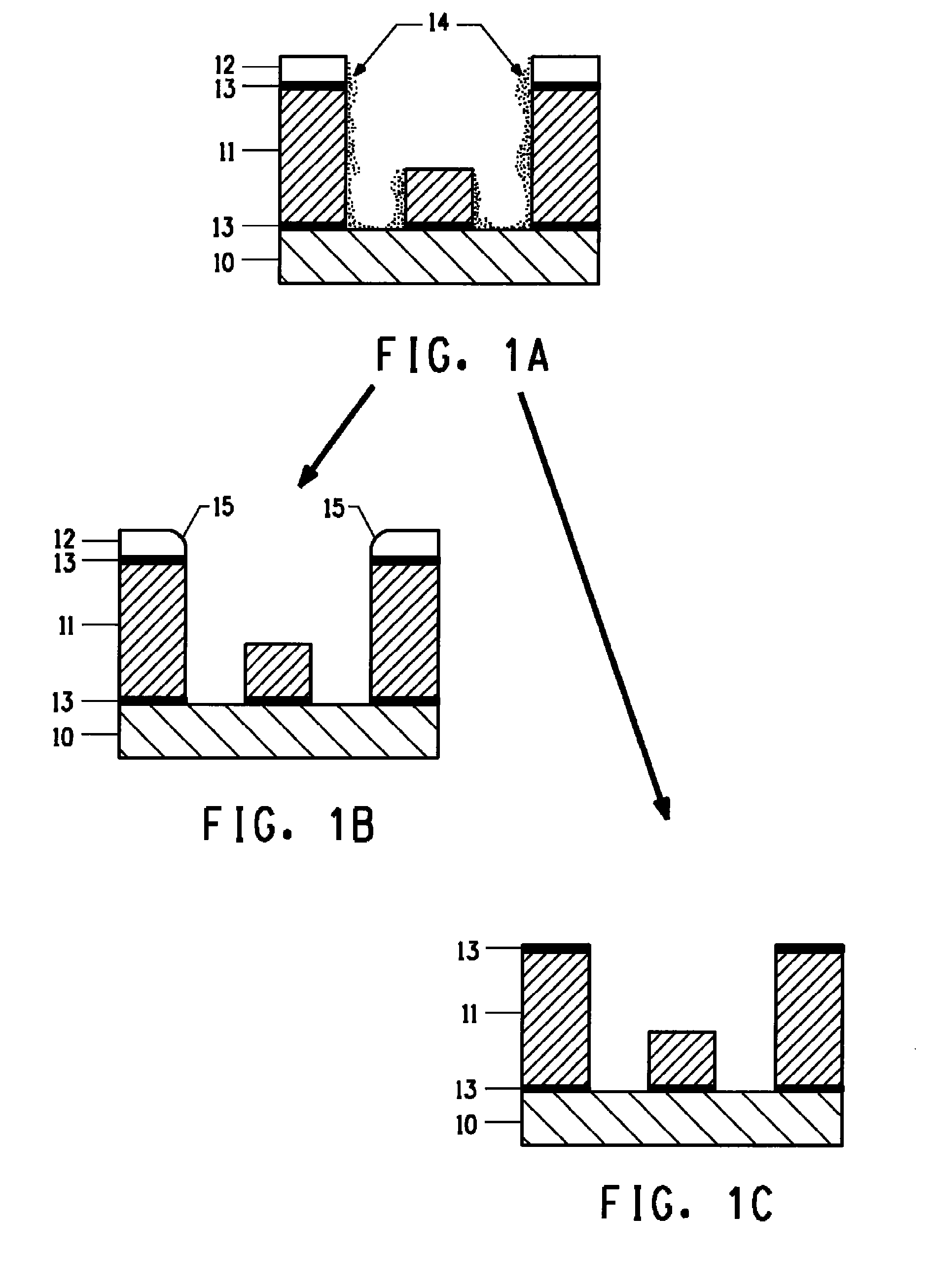
[0046]The compositions shown in Tables 1A & 1B and in Table 6A, 6B & 6C were prepared using water as the solvent, pyrazole as the Cu corrosion inhibitor, H2O2 as the oxidizing agent, and diglycolamine (DGA) as a base to adjust pH. (Water levels in the composition tables below are designated as “DI balance”, which means that water is present at a level such that the weight percent of all components, including water, is equal to 100 weight percent.) The compositions shown in Table 5A were prepared using water as the solvent, pyrazole as Cu corrosion inhibitor, H2O2 as the oxidizing agent, and glycolic acid (GA) to adjust pH. Composition pH can generally be adjusted using any suitable acid or base (i.e., proton source for acidic formulation or hydroxide source for basic formulat...


PUM


Abstract

A semiconductor processing composition and method for removing photoresist, polymeric materials, etching residues and copper oxide from a substrate comprising copper, low-k dielectric material and TiN, TiNxOy or W wherein the composition includes water, at least one halide anion selected from Cl or Br, and, where the metal hard mask comprises only TiN or TiNxOy, optionally at least one hydroxide source.

Description

INCORPORATION BY REFERENCE[0001]The entirety of U.S. patent application Ser. No. 13 / 209,859, filed on Aug. 15, 2011, is hereby expressly incorporated herein by reference.BACKGROUND OF THE INVENTION[0002]The presently disclosed and claimed inventive concept(s) relates to compositions and methods for cleaning integrated circuit substrates, and, more particularly, to compositions and methods comprising a halide anion which are effective in removing photoresist, post etch residue, and / or post planarization residue from substrates comprising copper, low-k dielectric material and metal hardmask, such as TiN, TiNxOy and W.[0003]Devices with critical dimensions on the order of 90 nanometers (nm) have involved integration of copper conductors and low-k dielectrics, and they require alternating material deposition processes and planarization processes. As the technology nodes advance to 45 nm and smaller, the decreasing size of semiconductor devices makes achieving critical profile control of...

Claims


Application Information

Patent Timeline
IPC IPC(8): H01L21/02C09K13/00
CPCH01L21/0206C09K13/00C11D3/0073C11D11/0047C11D3/3956C11D7/3281C11D3/3947H01L21/02063H01L21/31144H01L21/32134H01L21/31111
Inventor CUI, HUA
Owner EKC TECH
Why Eureka
Try Eureka