Mask blank, method of manufacturing the same, and transfer mask
- Summary
- Abstract
- Description
- Claims
- Application Information
AI Technical Summary
Benefits of technology
Problems solved by technology
Method used
Image

Examples
example 1
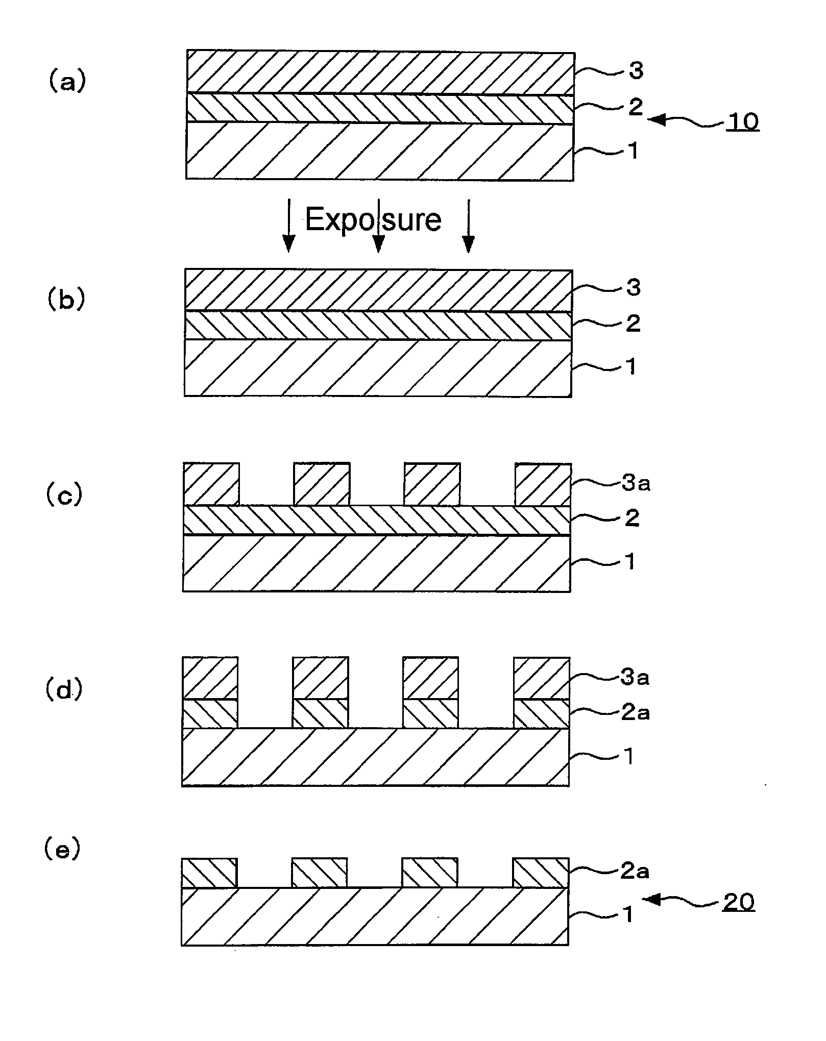
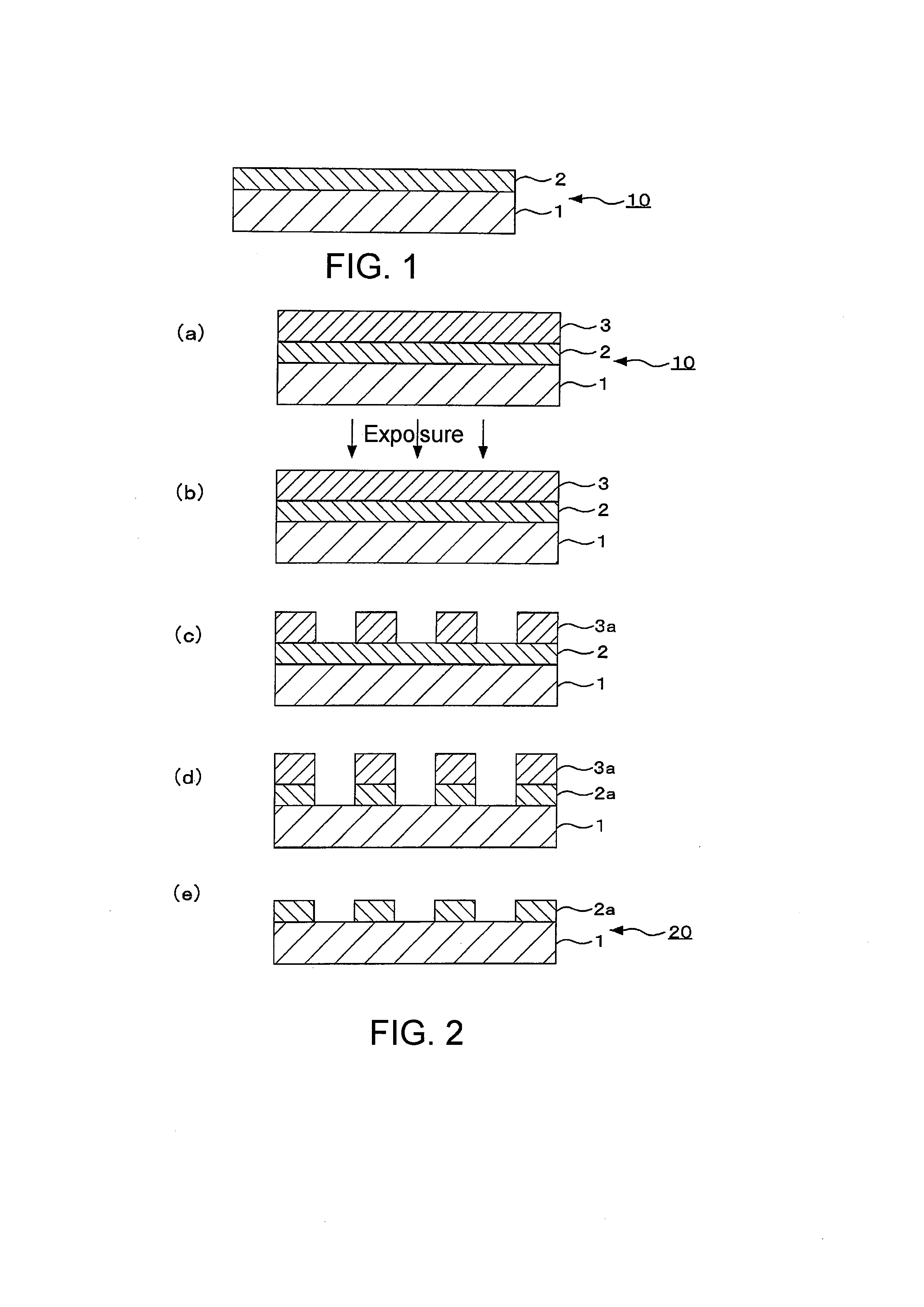
[0117]Using a synthetic quartz glass substrate having a 6-inch square size with a thickness of 0.25 inches as a transparent substrate, a light-semitransmissive film made of nitrided molybdenum and silicon was first formed on the transparent substrate.
[0118]Specifically, using a mixed target of molybdenum (Mo) and silicon (Si) (Mo:Si=10 mol %0:90 mol %), reactive sputtering (DC sputtering) was carried out by setting the power of a DC power supply to 3.0 kW in a mixed gas atmosphere of argon (Ar), nitrogen (N2), and helium (He) (gas flow rate ratio Ar:N2:He=5:49:46) at a gas pressure of 0.3 Pa, thereby forming a MoSiN film made of molybdenum, silicon, and nitrogen and having a thickness of 69 nm. Then, a heat treatment was applied to the substrate formed with the MoSiN film using a heating furnace in the atmosphere at a heating temperature of 450° C. for a heating time of 1 hour. The MoSiN film had a transmittance of 6.16% and a phase difference of 184.4 degrees for ArF excimer laser....
example 2
[0138]A phase shift mask blank was manufactured in the same manner as in Example 1 except that, in Example 1, the treatment time for causing the highly concentrated ozone gas (100 vol %) and the ethylene gas to act on the surface of the light-shielding film of the mask blank in which the light-semitransmissive film and the light-shielding film were laminated on the glass substrate was set to 30 minutes.
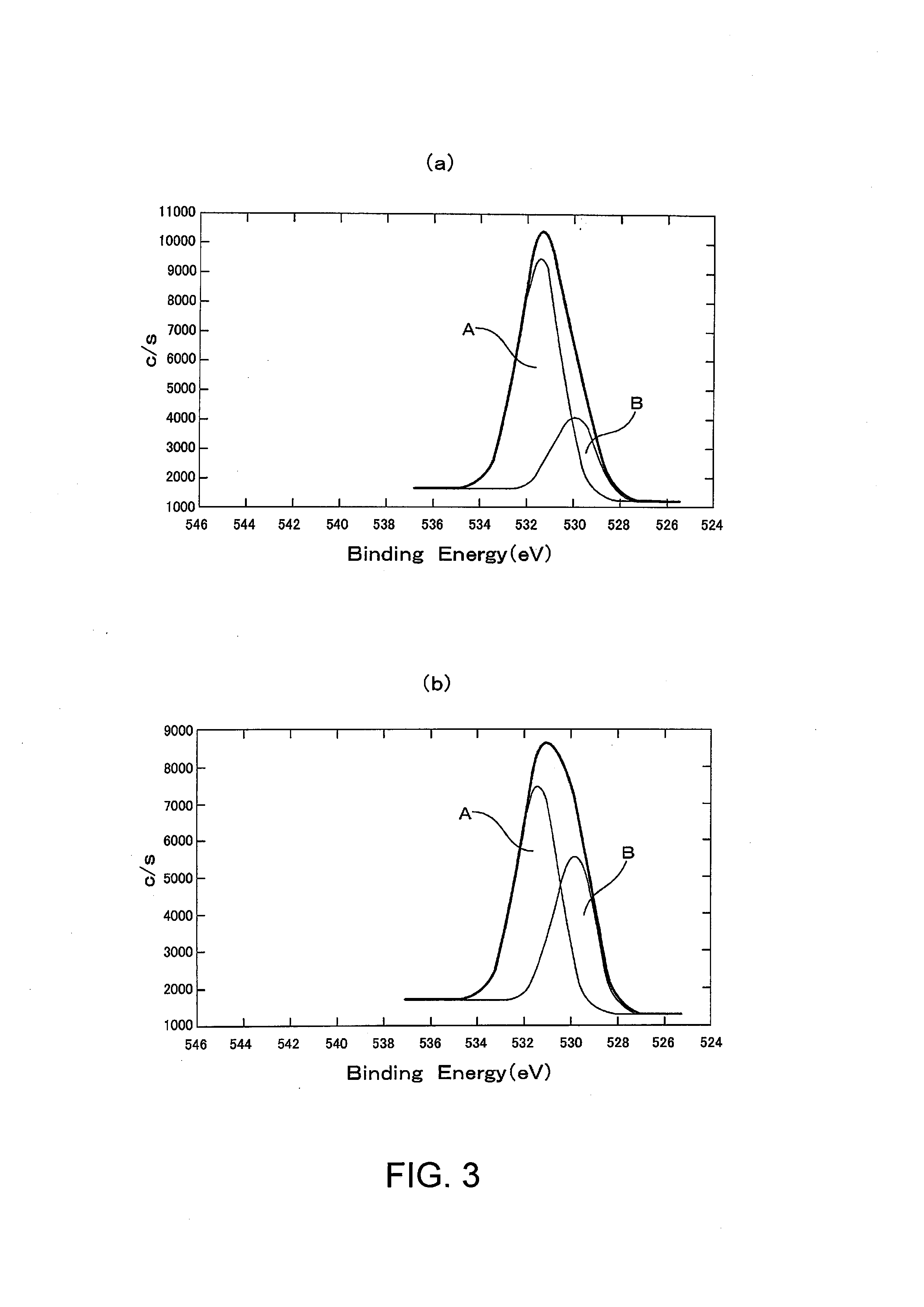
[0139]A section of the thin film of the laminated structure of the manufactured phase shift mask blank of this Example was observed in detail using TEM (transmission electron microscope). As a result, a coating film (surface modified layer) with a thickness of about 2 nm was formed at a surface layer portion of the light-shielding film. Further, the composition of this coating film was analyzed in detail using X-ray photoelectron spectroscopy by setting the inclination of a detector to 30° with respect to a surface. As a result, the elemental composition (at % ratio) was Cr:17.9, O:43...
example 3
[0146]Using a synthetic quartz glass substrate having a 6-inch square size with a thickness of 0.25 inches as a transparent substrate, a light-semitransmissive film, which was the same as that in Example 1, was formed on the transparent substrate, then heating was carried out, and then the following light-shielding film was formed.
[0147]Specifically, using a chromium (Cr) target as a sputtering target, reactive sputtering (DC sputtering) was carried out by setting the power of a DC power supply to 0.8 kW in a mixed gas atmosphere of argon (Ar), nitrogen (N2), and helium (He) (gas pressure 0.2 Pa, gas flow rate ratio Ar:N2:He=30:30:40), thereby forming a CrN layer having a thickness of 24 nm. Subsequently, reactive sputtering (DC sputtering) was carried out by setting the power of a DC power supply to 0.3 kW in a mixed gas atmosphere of argon (Ar), methane (CH4), nitrogen monoxide (NO), and helium (He) (gas pressure 0.3 Pa, gas flow rate ratio Ar+CH4:NO:He=65:3:40), thereby forming a...
PUM
 Abstract
Description
Claims
Application Information
 - Generate Ideas
- Intellectual Property
- Life Sciences
- Materials
- Tech Scout
- Unparalleled Data Quality
- Higher Quality Content
- 60% Fewer Hallucinations
Browse by: Latest US Patents, China's latest patents, Technical Efficacy Thesaurus, Application Domain, Technology Topic, Popular Technical Reports.
© 2025 PatSnap. All rights reserved.Legal|Privacy policy|Modern Slavery Act Transparency Statement|Sitemap|About US| Contact US: help@patsnap.com