Method and Apparatus for an Active Negative-Capacitor Circuit to Cancel the Input Capacitance of Comparators

a negative capacitance and comparator technology, applied in the field of active negative capacitance canceling circuits, can solve the problems of significant mismatches, false comparator outputs, and difficult design of high-performance circuits such as adc systems in integrated circuits, and achieve the effects of reducing the bandwidth of adc, reducing the headroom of analog integrated circuits, and reducing performan

Active Publication Date: 2014-03-06
TENSORCOM
View PDF8 Cites 12 Cited by
  • Summary
  • Abstract
  • Description
  • Claims
  • Application Information

AI Technical Summary

Benefits of technology

[0010]As the power supply voltage continues to reduce in the scaling of integrated circuits, the voltage headroom for analog integrated circuits decreases correspondingly. This makes the design of high performance circuits such as ADC systems in an integrated circuit much more challenging. Thus, the proper layout of comparators in an integrated circuit implementing an ADC is of great importance to overcome the mismatching condition. The comparators require that critical transistors, such as the input transistors, are matched to one another in terms of their local environment. The layout features of adjacent circuits can impact the behavior of a transistor in the current circuit by forming mismatches due to the various processing steps used to manufacture the integrated circuit. Increasing the length of the input transistors of the comparators helps to overcome this mismatch condition, but the input capacitance of the comparators increases and the performance decreases causing the bandwidth of the ADC to be reduced.
[0012]A simple layout technique is proposed in this embodiment that minimizes the concerns of the above aspects Instead of having extra dummy fingers for each comparator to reduce the mismatch within one comparator between input transistors, the comparators are aligned right next to each other, so that all the input transistors share one whole active area. Thereby, the fingers on the edge of the active area serve as the dummy fingers for the neighboring comparators.
[0013]In another embodiment, the core concept of this ADC is the high-speed folly-differential comparators which are clocked at 2640 MHz that is used in the 60 GHz transceiver. Basically, each comparator consists of four parts; a pre-amplifier stage which samples and amplifies the input signal from the preceding stage or Programmable Gain Amplifier (PGA); a capture stage that is clocked to capture the contents of the pre-amplifier stage, a pair of clocked cross-coupled transistors which regenerates the small signal to nearly a rail-to-rail signal; and an output latch which latches up the previous results after regeneration for application to the following static CMOS circuits. The pre-amplifier stage is not clocked; therefore, the pre-amplifier stage does not suffer initialization and transient behavior effects. Instead, a capture stage uses the clock signal to transfer the contents of the pre-amplifier stage into a memory regeneration stage. The capture stage is clocked by pulses that, are timed to minimize the clock kick-back generated by the memory regeneration stage.
[0014]In another embodiment, since a flash ADC converter is used, a number of comparators are placed in parallel with their inputs connected together. The clock kick-back from the many pre-amplifier stages to the PGA is significantly reduced by incorporating the use of a clock-less pre-amplifier stage. Since the clocking occurs after the pre-amplifier stage in the capture and memory regeneration stages, the capture stage isolates the clock kick-back from proceeding into the pre-amplifier stage. In addition, because the pre-amplifier stages are not clocked, their transient response of being enabled and disabled is eliminated thereby reducing this portion of the clock kick-back of the pre-amplifier stage. Thus, the clock kick-back is inventively reduced even when 17 comparators are driven simultaneously by one differential signal source by addressing several the above aspects in this design.
[0015]The differential output of the PGA is loaded by the input differential gate capacitance of 17 comparators. Differential metal layer traces are used to interconnect these 17 comparators to the PGA. Both the input capacitance of the comparators and the capacitance of the metal layer trace add together to increase the differential capacitive load. The differential capacitive load presented to the PGA is quite large and reduces the bandwidth of this signal path. Thus, this implies that the input, differential pair of transistors in the comparator should not be excessively large in width in order to minimize the input capacitance and reduce the corresponding power dissipation. However, the embodiment presented in this inventive idea allows the input gates of the comparator to have large width transistors which overcomes the performance degradation due to capacitance mentioned above in the ADC comparator. The inventive idea uses an active negative-capacitor circuit to cancel the effect of the large input capacitance of the comparators. This cancellation minimizes the capacitance between the PGA and ADC and extends the gain characteristics of the interface between the PGA's output and the inputs of the first stage of the comparators. The active negative-capacitance, basically, is a cross pair NMOS with a capacitor connecting their sources, and each NMOS is biased by a current source.

Problems solved by technology

This makes the design of high performance circuits such as ADC systems in an integrated circuit much more challenging.
The layout features of adjacent circuits can impact the behavior of a transistor in the current circuit by forming mismatches due to the various processing steps used to manufacture the integrated circuit.
Mismatches between transistors, especially input transistor pairs, will lead to false comparator outputs.
In addition, improper layout may lead to significant mismatches both within one comparator and between identical comparators during manufacture.
Both mismatches may result in the ADC making false decisions.
Furthermore, a poorly packed layout design will add unnecessary interconnect trace lengths for both signal and clock, especially for an ADC with large number of comparators.
These longer trace interconnects, implemented as a differential signal that has parallel routings, will dramatically degrade the bandwidth of the system.
The longer clock routing requires larger clock buffers which increase the overall power consumption, and more profoundly, additional clock jitter will occur, which will cause problems such as bubbles in the decoded results and lower ENOB (Effective Number of Bits).
The longer power supply lines introduce additional IR drops, which further contribute to the mismatches among different comparators.

Method used


Image

  • Method and Apparatus for an Active Negative-Capacitor Circuit to Cancel the Input Capacitance of Comparators
  • Method and Apparatus for an Active Negative-Capacitor Circuit to Cancel the Input Capacitance of Comparators
  • Method and Apparatus for an Active Negative-Capacitor Circuit to Cancel the Input Capacitance of Comparators

Examples


Embodiment Construction

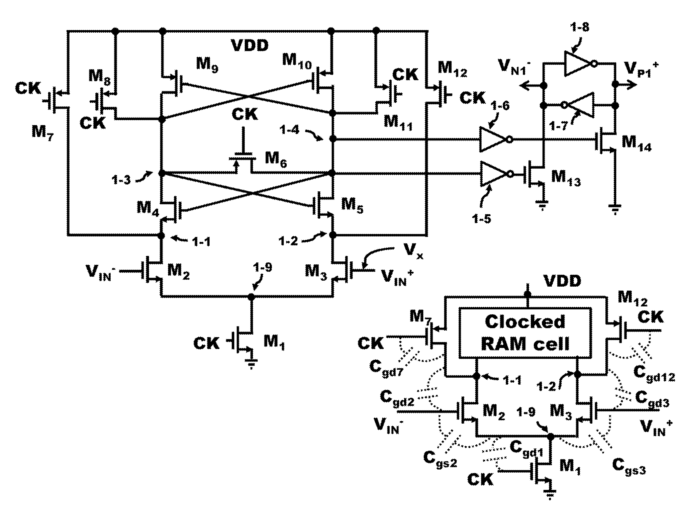
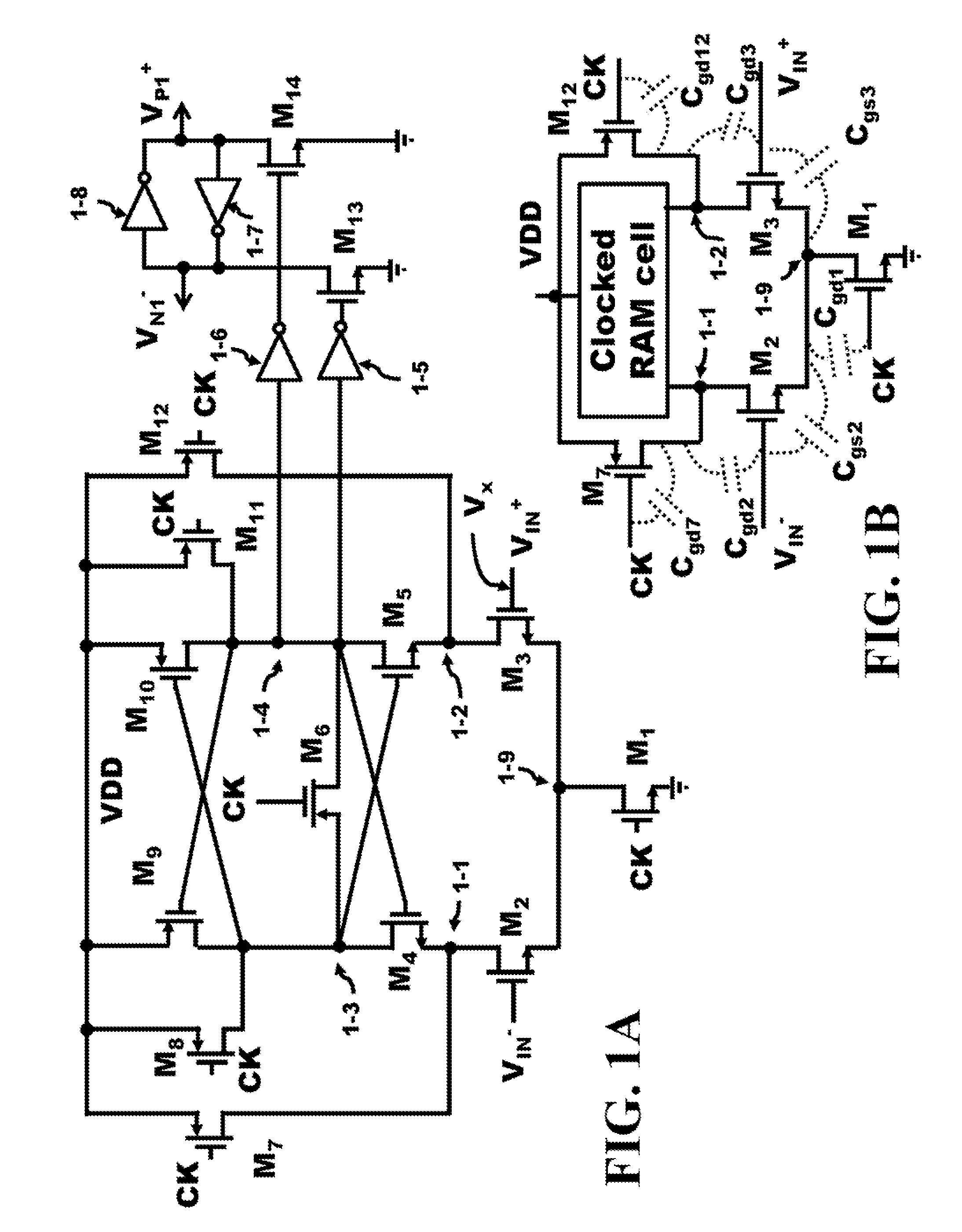
[0039]The inventions presented in this specification can be used in any wired or wireless system or any low power supply voltage design. The techniques are applicable to any amplifier design, ADC design, or PGA and ADC interface design. These techniques can be extended to other circuit designs where an increased bandwidth between two interfaces, a clock kick-back reduction, or a matched transistor within a circuit is required.

[0040]A comparator that is clocked in the first pre-amplifier stage is illustrated in FIG. 1A. The basic construction of the clocked pre-amplifier stage includes a ground switch M1 with a gate coupled to a clock CK. The drain of M1 1-9 is coupled to the source of two N-channel transistors M2 and M3. M2 is driven by VIN− while M3 is driven by the other differential input signal VIN+. The drain of M2 is coupled to 1-1 and is also coupled to the drain of P-channel transistor M2 controlled by the same clock CK. The drain of transistor M3 1-2 is coupled to the drain...


PUM


Abstract

The differential output of a Programmable Gain Amplifier (PGA) is loaded by the input differential gate capacitance of a plurality of Analog to Digital converters (ADC) comparators and the differential metal layer traces to interconnect these comparators to the PGA. The differential capacitive load presented to the PGA is quite large and reduces the bandwidth of this interconnect between the PGA and ADC. To overcome the performance degradation due to the differential capacitive load, an active negative-capacitor circuit cancels the effect of the large input capacitance of the ADC comparators. This cancellation extends the gain characteristics of the interconnect between the PGA's output and the inputs of the first stage of the comparators. The active negative-capacitance is comprised of a cross pair NMOS with a capacitor connecting their sources where each NMOS is biased by a current source.

Description

CROSS-REFERENCE TO RELATED APPLICATIONS[0001]The present application is related to the co-filed U.S. application entitled “Method and Apparatus for Reducing the Clock Kick-Back of ADC Comparators While Maintaining Transistor Matching Behavior” filed on Sep. 3, 2012, which is invented by the same inventor as the present application and incorporated herein by reference in their entireties.BACKGROUND OF THE INVENTION[0002]The Federal Communications Commission (FCC) has allotted a spectrum of bandwidth in the 60 GHz frequency range (57 to 64 GHz). The Wireless Gigabit Alliance (WiGig) is targeting the standardization of this frequency band which will support data transmission rates up to 7 Gbps. Integrated circuits, formed in semiconductor die, offer high frequency operation in this millimeter wavelength range of frequencies. Some of these integrated circuits utilize Complementary Metal Oxide Semiconductor (CMOS), Silicon-Germanium (SiGe) or Gallium Arsenide (GaAs) technology to form th...

Claims


Application Information

Patent Timeline
Patent Type & Authority Applications(United States)
IPC IPC(8): H03H11/44
CPCH03H11/481H03K5/2481H03M1/002H03M1/0836H03M1/0845H03M1/183
Inventor DAI, DAI
Owner TENSORCOM
Why Eureka
Try Eureka