High efficiency ultraviolet light emitting diode with band structure potential fluctuations

a technology of ultraviolet light and band structure, applied in the direction of semiconductor/solid-state device manufacturing, electrical apparatus, semiconductor devices, etc., can solve problems such as band structure potential fluctuations, and achieve the effects of optimizing electron injection, high output, and high efficiency

Active Publication Date: 2014-04-17
TRUSTEES OF BOSTON UNIV
View PDF3 Cites 117 Cited by
  • Summary
  • Abstract
  • Description
  • Claims
  • Application Information

AI Technical Summary

Benefits of technology

[0011]The present invention provides methods for fabricating UV LEDs of high efficiency and high output, and emitting over the range from 200 nm to 365 nm, for use in water purification, surface sterilization, free space non-line-of-sight communications, information storage and retrieval, epoxy curing, medical therapy, and a variety of electronic devices. The methods involve growth of AlGaN semiconductor material under conditions of excess gallium, which covers the surface of the growing film with liquid gallium and changes the growth mode from vapor phase epitaxy to liquid phase epitaxy. This leads to lateral compositional inhomogeneities and thus band structure potential fluctuations due to statistical fluctuations of the thickness of liquid gallium on the surface of the growing film. The invention also provides designs for UV LED construction which avoid cracks in the AlGaN material, optimize the injection of electrons and holes, and maximize light output. The LEDs according to the invention achieve high internal and external quantum efficiency.

Problems solved by technology

This leads to lateral compositional inhomogeneities and thus band structure potential fluctuations due to statistical fluctuations of the thickness of liquid gallium on the surface of the growing film.

Method used


Image

  • High efficiency ultraviolet light emitting diode with band structure potential fluctuations
  • High efficiency ultraviolet light emitting diode with band structure potential fluctuations
  • High efficiency ultraviolet light emitting diode with band structure potential fluctuations

Examples


example 1

Growth of AlGaN Layers by Plasma Assisted MBE

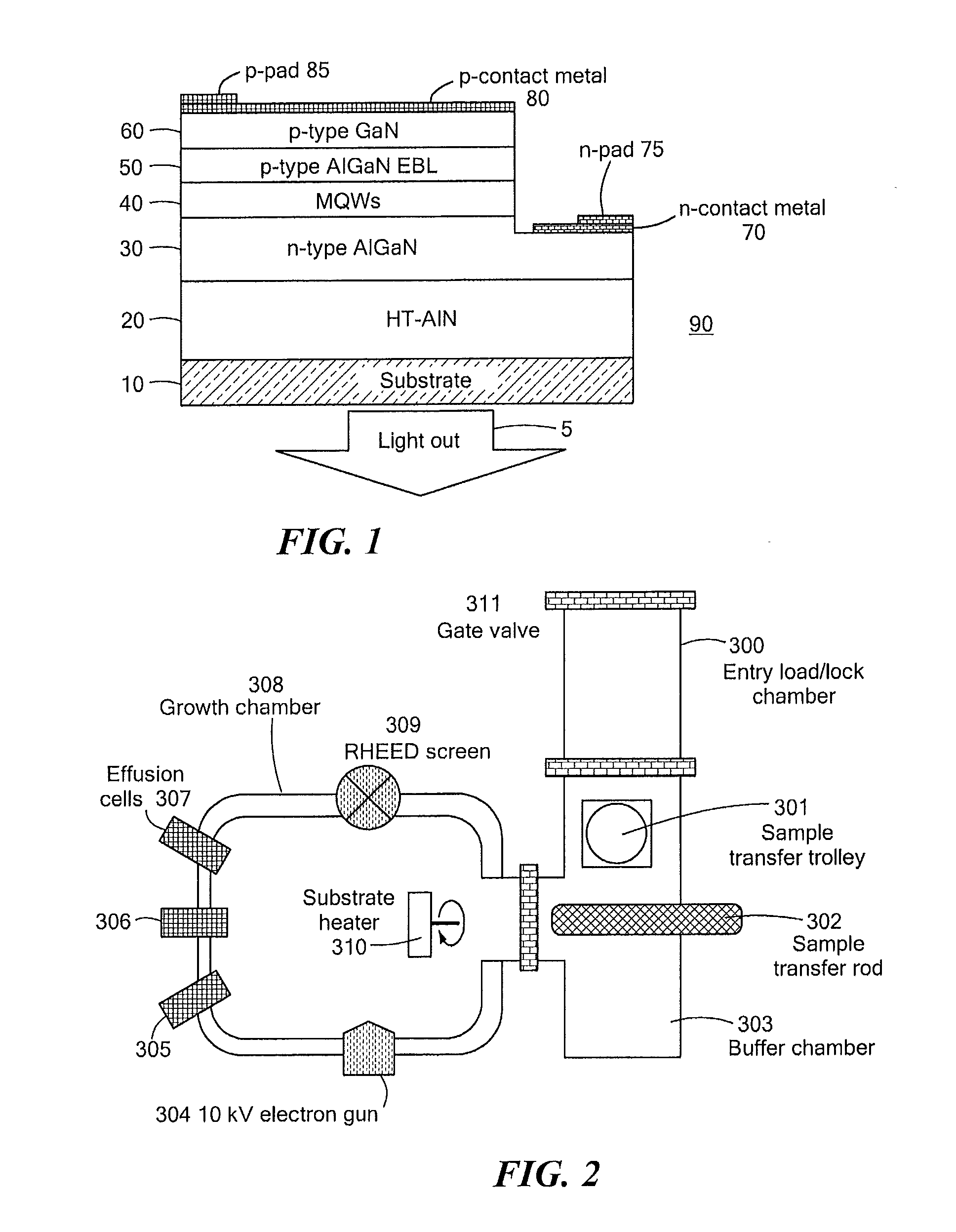
[0235]Plasma assisted MBE was used to deposit high quality single crystal epitaxial films of III-nitrides. The GenII MBE system used is depicted schematically in FIG. 2. Epitaxial growth was performed in an ultra high vacuum (UHV) environment (typically at 10−10 Torr), and therefore the background impurity level incorporated in the film was effectively reduced. The epitaxy proceeded by impinging“molecular beams” of constituent elements on the growth surface, where they arrive, diffuse, reevaporate and finally incorporate into the growing film. The molecular beams were supplied by heating furnaces (effusion cells 305, 306, 307, one for each metallic element, e.g., gallium, aluminum, and indium), where high purity pallets of the respective materials were stored in pyrolytic boron nitride crucibles, and heated up to their sublimation temperatures. Growth proceeded in the molecular flow regime in which evaporated atoms do not interact with ea...

example 2

Analysis of AlGaN Films and Semiconductor Structures

[0239]The III-nitride films and devices produced by plasma-assisted MBE were characterized by SEM and AFM imaging, X-ray diffraction, photoluminescence, cathode luminescence, and / or electroluminescence. A Zeiss Supra 40VP system was used for SEM imaging, and a Digital Instrument Dimension 3100 instrument was used for AFM For AFM, all samples were measured in the tapping mode using a Si etched SPM probe from Mikromasch. A Philips four-circle high resolution diffractometer was used for X-ray diffraction. The sample stage was able to rotate in three planes (ω, ψ, and χ), and the detector could rotate in the θ plane. Photoluminescence (PL) was used to evaluate the luminescence properties of the AlGaN materials, especially MQWs. The electron-hole pairs were generated by a laser. The emission profile was obtained by exciting the sample with photons above the optical band gap of the material. To excite AlGaN alloys emitting in the wavelen...

example 3

Fabrication of LED Devices

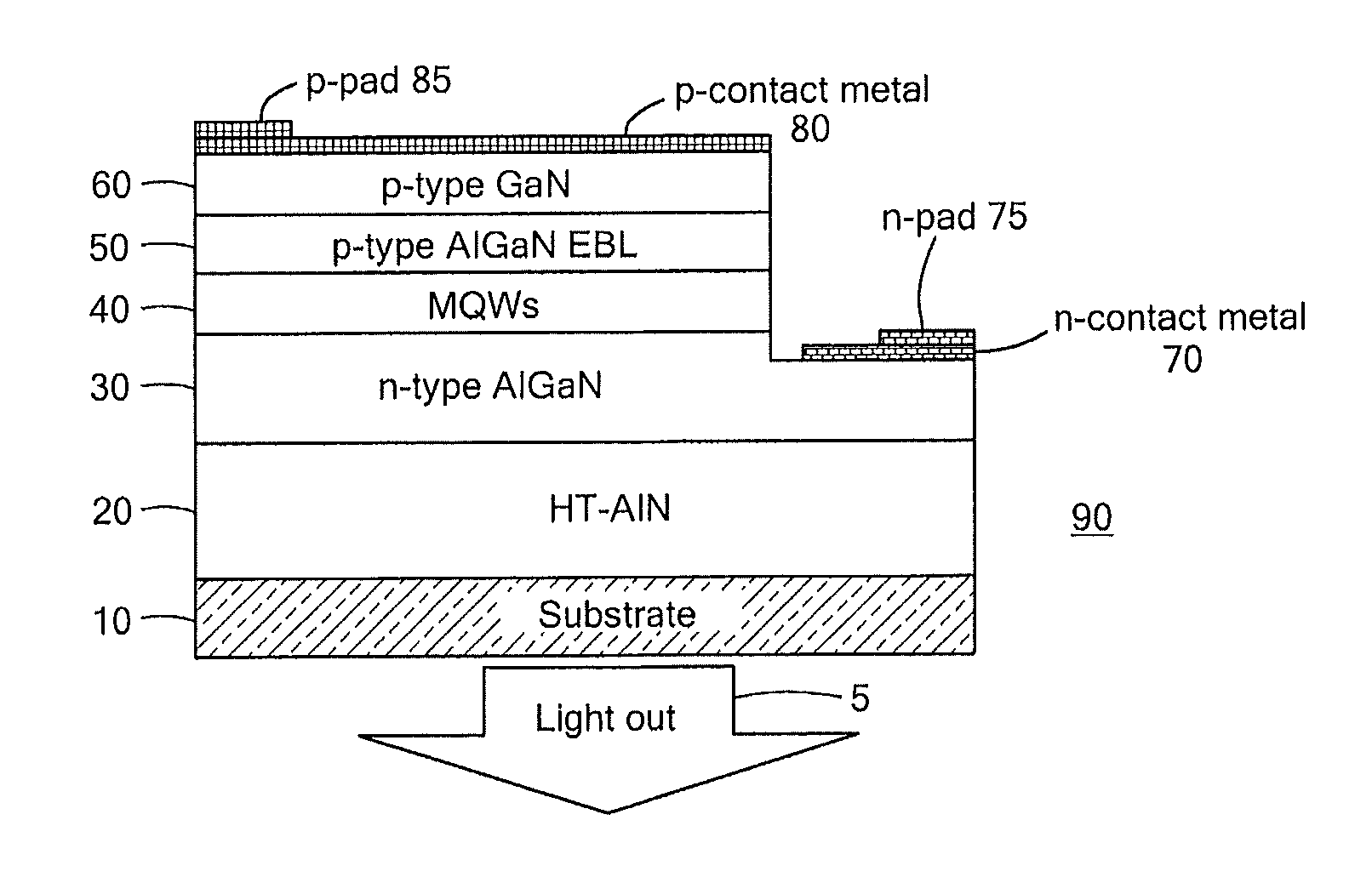
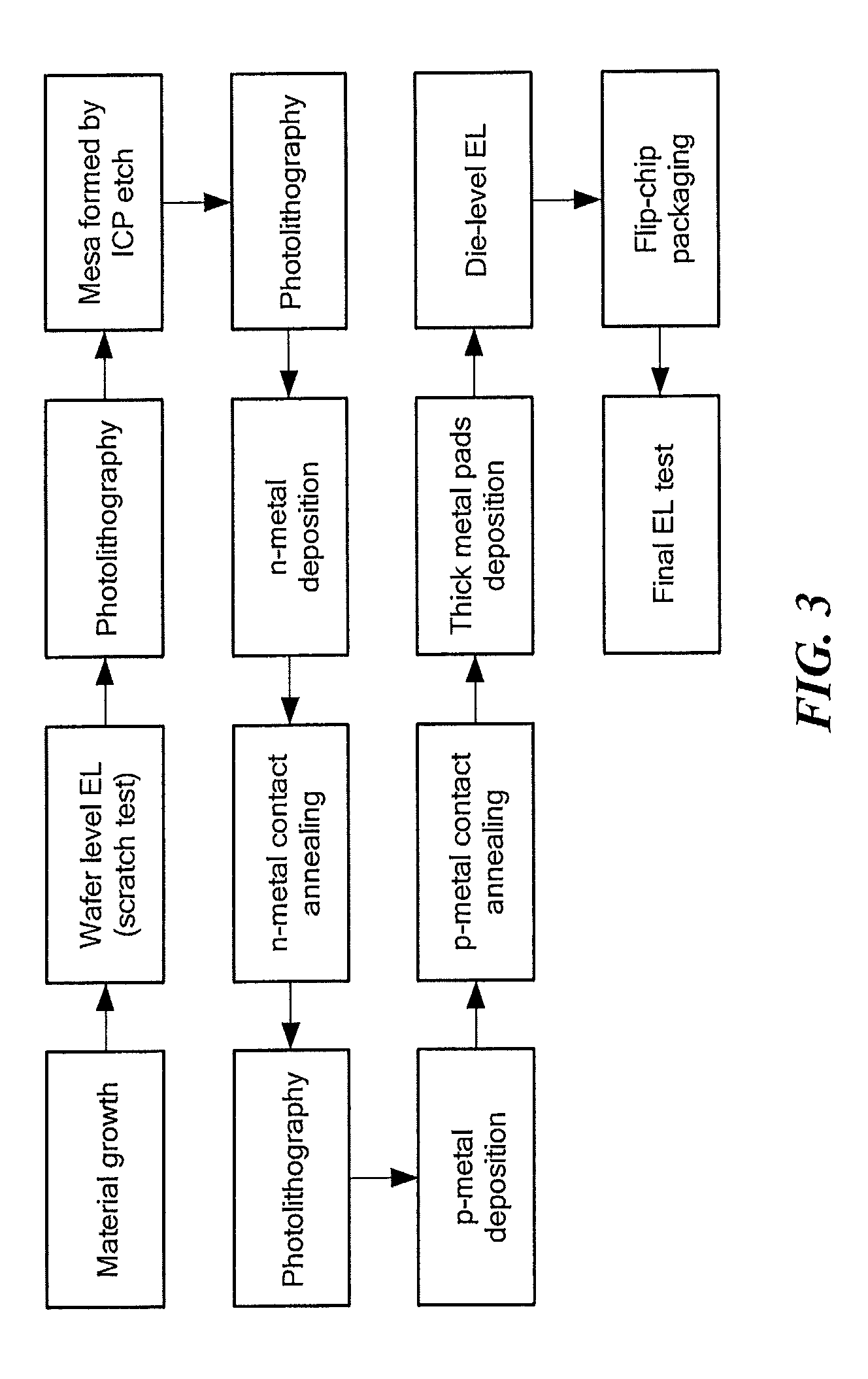
[0240]Light emitting diodes were fabricated from epitaxial films grown on sapphire substrates by standard device process techniques. LEDs with mesa-etched geometry designed for bottom light collection from the backside of the sapphire substrate were produced and their performance measured, as described in examples which follow. The electroluminescence (EL) properties of deep UV LEDs were obtained, including I-V characteristics, power spectra and L-I characteristics. Some devices were flip-chip packaged onto Si or AlN submounts. An overview of the fabrication process is presented in FIG. 3.


PUM


Abstract

A method of growing an AlGaN semiconductor material utilizes an excess of Ga above the stoichiometric amount typically used. The excess Ga results in the formation of band structure potential fluctuations that improve the efficiency of radiative recombination and increase light generation of optoelectronic devices, in particular ultraviolet light emitting diodes, made using the method. Several improvements in UV LED design and performance are also provided for use together with the excess Ga growth method. Devices made with the method can be used for water purification, surface sterilization, communications, and data storage and retrieval.

Description

CROSS REFERENCE TO RELATED APPLICATIONS[0001]This application claims the priority of U.S. Provisional Application No. 61 / 329,947 filed Apr. 30, 2010 and entitled, METHOD OF GROWING AlGaN LAYER WITH BAND STRUCTURE POTENTIAL FLUCTUATIONS AND MANUFACTURING ULTRAVIOLET LIGHT EMITTING DEVICES CONTAINING THE SAME, which is incorporated by reference herein.STATEMENT REGARDING FEDERALLY SPONSORED RESEARCH OR DEVELOPMENT[0002]The work leading to this invention was carried out with United States Government support provided under Contract No. W911NF-06-2-0040 awarded by United States Army Research Lab. Thus, the United States Government has certain rights in this invention.BACKGROUND[0003]The bandgap of III-nitride materials, including (Al, Ga, In)—N and their alloys, extends from the very narrow gap of InN (0.7 eV) to the very wide gap of AlN (6.2 eV), making them highly suitable for optoelectronic applications such as light emitting diodes (LEDs), laser diodes, optical modulators, and detect...

Claims


Application Information

Patent Timeline
Patent Type & Authority Applications(United States)
IPC IPC(8): H01L33/32H01L33/06H01L33/00
CPCH01L33/32H01L33/06H01L33/0075H01L21/0237H01L21/0242H01L21/02458H01L21/02507H01L21/0254H01L21/02573H01L21/0259H01L21/02625H01L33/007H01L33/025H01L33/14
Inventor LIAO, YITAOMOUSTAKAS, THEODORE D.
Owner TRUSTEES OF BOSTON UNIV
Why Eureka
Try Eureka