Copper(i) complexes for optoelectronic devices

Active Publication Date: 2014-08-21
SAMSUNG DISPLAY CO LTD
View PDF0 Cites 3 Cited by
  • Summary
  • Abstract
  • Description
  • Claims
  • Application Information

AI Technical Summary

Problems solved by technology

Moreover, a large number of OLED emitter materials known to date are ecolo...

Method used


Image

  • Copper(i) complexes for optoelectronic devices
  • Copper(i) complexes for optoelectronic devices
  • Copper(i) complexes for optoelectronic devices

Examples


example 1

[0107]The appropriate N∩L ligand (1.00 mmol, 1.00 eq.), [Cu(CH3CN)4]PF6 (10) (1.00 mmol, 1.00 eq.) and the L-B-L ligand (1.00 mmol, 1.00 eq.) were dissolved in 10 mL solvent mixture consisting of dichloromethane:ethanol=3:1 under nitrogen atmosphere and stirred for 4 h. The complex was purified by precipitation in diethyl ether, filtered, washed with diethyl ether and dried.

[0108]The complex obtained above (0.05 mmol, 1.00 eq.) and KOH (7.75 mmol, 15.0 eq.) were dissolved in 5 mL methanol under nitrogen atmosphere and stirred for 6 h. Subsequently, the solvent was removed in vacuo, the residue extracted with DCM and filtered. After removal of the solvent the complex was obtained as a white powder.

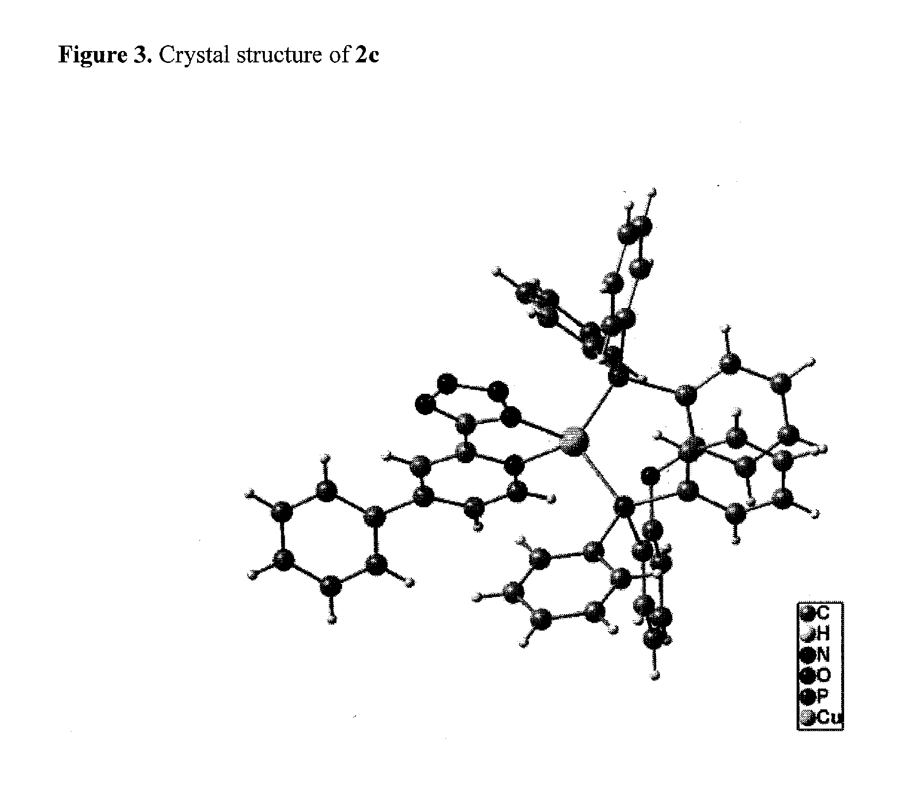
2c: L-B-L=Bis(diphenylphosphine)diphenylether:

Characterization:

[0109]Elemental analysis: C48H36CuN5OP2 (823.17): calc. C, 69.94; H, 4.40; N, 8.50.

[0110]found C, 69.41; H, 4.47; N, 8.00.

[0111]MS (FAB), m / z (%): 1423 (3) [LCu2(P̂P)2], 1139 (1) [Cu(P̂P)2], 888 (1) [LCu2P̂P], 860 (6) [LCu2P̂P—N...

example 2

[0137]The N∩L ligand (1.00 mmol, 1.00 eq.) was dissolved in 10 mL dichloromethane under nitrogen atmosphere, an equimolar amount of base added and stirred for 1 hour. Then an equimolar amount of Cu(CH3CN)4]BF4 was added, stirred for 1 hour, an equimolar amount of the appropriate L-B-L ligand added and stirred over night. The complex was purified by precipitation in diethyl ether, filtered, washed with diethyl ether and dried.

[0138]4a: L-B-L=2× PPh3:

[0139]Characterization:[0140]The emission lifetime of 4a is 0.8 μs (Horiba Fluoromax 4 with TCSPC).

[0141]4c: L-B-L=Bis(diphenylphosphine)diphenylether

[0142]Characterization:[0143]The emission spectrum of 4c at 298 K is shown in FIG. 9.[0144]The emission spectrum of 4c at 77 K is shown in FIG. 9.[0145]The emission quantum yield of 4c is 65% (measured with Hamamatsu C9920-02G).[0146]The emission lifetime of 4c is 1.0 μs (Horiba Fluoromax 4 with TCSPC).[0147]The ΔE(S1-T1) value of 4c is 169 cm−1 (determined by measuring the temperature depen...

example 3

[0151]The synthesis was carried out as mentioned in example 2.

[0152]6c: L-B-L=Bis(diphenylphosphin)diphenylether:

[0153]Characterization:

[0154]MS (FAB), m / z (%): 2195 (1) [L2Cu3(P̂P)3], 1917 (1) [L3Cu4(P̂P)2], 1660 (1) [L2Cu3(P̂P)2], 1400 (10) [LCu2(P̂P)2], 1140 (2) [Cu(P̂P)2], 860 (5) [LCu2(P̂P)], 798 (4) [LCuP̂P], 741 (6) [LCuP̂P—N4], 602 (100) [CuP̂P].[0155]The emission spectrum of 6c at 298 K is shown in FIG. 10.[0156]The emission quantum yield of 6c is 20% (measured with Hamamatsu C9920-02G).[0157]The emission lifetime of 6c is 0.7 μs (Horiba Fluoromax 4 with TCSPC).

[0158]6e: L-B-L=(Oxybis(3-methyl-6,1-phenylene))bis(diphenylphosphine):

[0159]Characterization:

[0160]MS (FAB), m / z (%): 2278 (1) [L4Cu6(P̂P)2—CH3], 1713 (2) [L2Cu3(P̂P)2], 1455 (12) [LCu2(P̂P)2], 1196 (1) [Cu(P̂P)2], 889 (7) [LCu2(P̂P)], 825 (2) [LCuP̂P], 769 (3) [LCuP̂P—N4], 739 (2) [LCuP̂P—N4—(CH3)2], 692 (2) [Cu2P̂P], 629 (100) [CuP̂P], L: tetrazole ligand, P̂P: phosphine ligand.

[0161]The emission spectrum of 6e at...


PUM


Abstract

Copper(I) complexes for the emission of light with a structure according to formula A:
wherein:
    • M is Cu(I);
    • L-B-L: a neutral, bidentate ligand,
    • Z4-Z7: includes N or the fragment CR,
    •  with R=organic group, selected from the group consisting of: hydrogen, halogen or deuterium or groups which are bound via oxygen (—OR′″), nitrogen (—NR′″2), or phosphorous atoms (PR′″2) as well as alkyl, aryl, heteroaryl, alkenyl, alkinyl, trialkylsilyl and triarylsilyl groups or substituted alkyl, aryl, heteroaryl and alkenyl groups with substituents such as halogens or deuterium or lower alkyl groups;
    • X is either CR′″2 or NR′″;
    • Y is either O, S or NR′″;
    • Z8 includes the fragment CR′,
    •  with R′═O*R′″, N*R′″2 or P*R′″2, wherein the bond to the Cu atom is carried out via these groups;
    • R″ is a sterically demanding substituent, which inhibits a change in geometry in direction to planarization of the complex in excited state,
    • R′″=organic group which is selected from the group consisting of: hydrogen, halogen or deuterium, as well as alkyl, aryl, heteroaryl, alkenyl, alkinyl groups or substituted alkyl, aryl, heteroaryl and alkenyl groups with substituents such as halogens or deuterium, alkyl groups, and further generally known donor and acceptor groups
    • * indicates the atom which receives the complex bond; and
    • # indicates the atom which mediates the bond with the second chemical unit.

Description

[0001]The present invention relates to the use of soluble copper(I) complexes (Cu(I)-complexes) as emitters in OLEDs (organic light emitting diodes) and in other optoelectronic devices.INTRODUCTION[0002]In principle, OLEDs are outstandingly suitable for the production of large-area illumination and display applications but can be found only in devices of small format at the moment due to extensive production methods. OLEDs are generally implemented in layer structures. For better understanding, FIG. 1 shows a basic structure of an OLED. Owing to the application of external voltage to a transparent indium tin oxide (ITO) anode and a thin metal cathode, the anode injects positive holes, and the cathode negative electrons. These differently charged charge carriers pass through intermediate layers, to which also hole or electron blocking layers not shown here may belong, into the emission layer. The oppositely charged charge carriers meet therein at or close to doped emitter molecules, ...

Claims


Application Information

Patent Timeline
IPC IPC(8): H01L51/00H01L51/56
CPCH01L51/0091H01L2251/10H01L51/56C09K11/06C09K2211/1007C09K2211/1029C09K2211/1044C09K2211/1048C09K2211/1051C09K2211/1059C09K2211/188Y02E10/549C07F9/5045C07F1/005H10K85/371H10K50/11H10K2101/10C07F1/08Y02B20/00H10K71/00
Inventor BAUMANN, THOMASGRAB, TOBIASBERGMANN, LARISSA
Owner SAMSUNG DISPLAY CO LTD
Why Eureka
Try Eureka