Selective etching of a matrix comprising silver NANO wires

a silver nano wire and selective etching technology, applied in the direction of surface treatment compositions, non-conductive materials with dispersed conductive materials, chemistry apparatuses and processes, etc., can solve the problems of time-consuming and expensive, material-intensive, time-consuming and expensive etching methods, etc., to achieve high throughput and cost-effective

Inactive Publication Date: 2014-10-02
MERCK PATENT GMBH
View PDF5 Cites 7 Cited by
  • Summary
  • Abstract
  • Description
  • Claims
  • Application Information

AI Technical Summary

Benefits of technology

[0045]Therefore, the objective of the present invention is to provide a new etching composition, which is suitable to be employed in a simplified etching method for polymer-surfaces. It is also an objective of the present invention to provide an improved etching method for polymer-surfaces, which can be carried out with throughputs as high as possible, and which is significantly less expensive than conventional wet and dry etching methods in the liquid or gas phase.
[0117]Significant advantages in the present compositions arise, in particular, through an outstanding screen-printing behaviour, enabling continuous printing of surfaces to be treated without interruptions. The use of the etching pastes according to the invention enables surprisingly fine etching structures since the pastes have high viscosities on addition of a thickener in the presence of polymer particles. This enables the pastes to be applied in printing with a high paste layer and consequently for the layers to be etched deep, because the achieved printed height under printing conditions causes a delayed drying of the printed etching species. This enables the etching species to act on the substrate for a longer time. This is particularly important in the case of etching under elevated temperatures. In addition, the material remaining after the etching process can be removed easily in the final cleaning step and the good rinsing behaviour after etching leads to a short subsequent cleaning.

Problems solved by technology

The wet-chemical and dry etching methods include material-intensive, time-consuming and expensive process steps:A. masking of the areas not to be etched, for example by photolithography:production of a negative or positive of the etch structure (depending on the resist), coating of the substrate surface (for example by spin-coating with a liquid photoresist),drying of the photo-resist, exposure of the coated substrate surface, development, rinsing, if desired dryingB. etching of the structures by:dip methods (for example wet etching in wet-chemical banks):dipping of the substrates into the etch bath, etching process, repeated rinsing in H2O cascade basins, dryingspin-on or spray methods:the etching solution is applied to a rotating substrate, the etching operation can take place without / with input of energy (for example IR or UV irradiation),or known dry-etching methods as there are for example, plasma etching in expensive vacuum units or etching with reactive gases in flow reactors andC.
Since these etching methods are time consuming and expensive, experiments were carried out to etch AgNW comprising layers by exposure to applied pasty etching compositions at elevated temperatures or by exposure of thermal radiation or infrared radiation.

Method used


Image

  • Selective etching of a matrix comprising silver NANO wires
  • Selective etching of a matrix comprising silver NANO wires

Examples


example 1

Best Mode

[0133]15 g Ethylenglycolmonobutylether

[0134]15 g Triethylenglycolmonomethylether

[0135]29 g Polycarbonat

[0136]72 g Ameisensaure

[0137]30 g DI Water

[0138]16 g Ammoniumhydrogendifluorid

[0139]46 g Polyvinylpyrrolidon (PVP) K-120

[0140]60 g Vestosint 2070

[0141]The compounds are successively mixed with each other. After standing for some hours the paste can be printed.

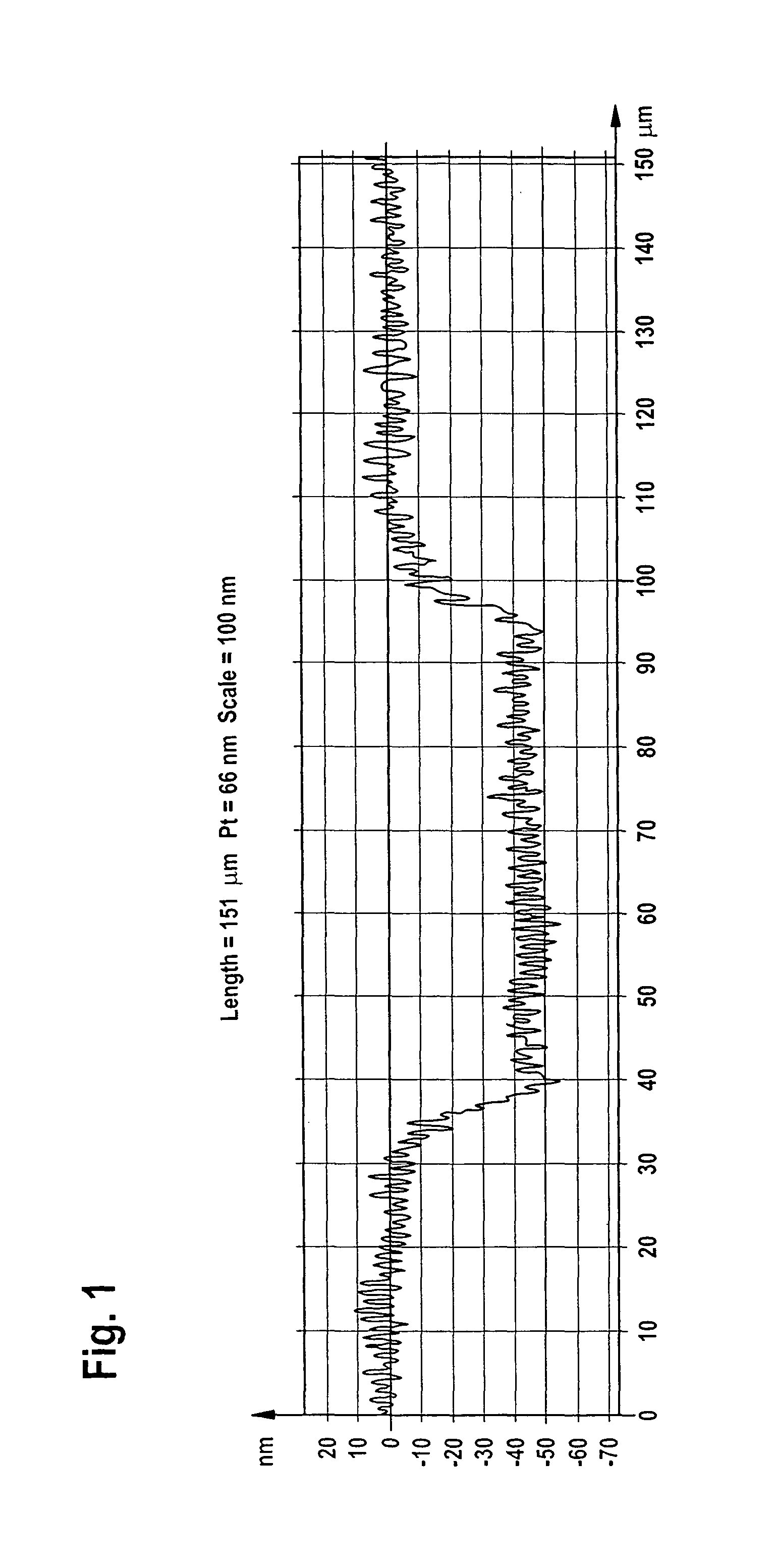
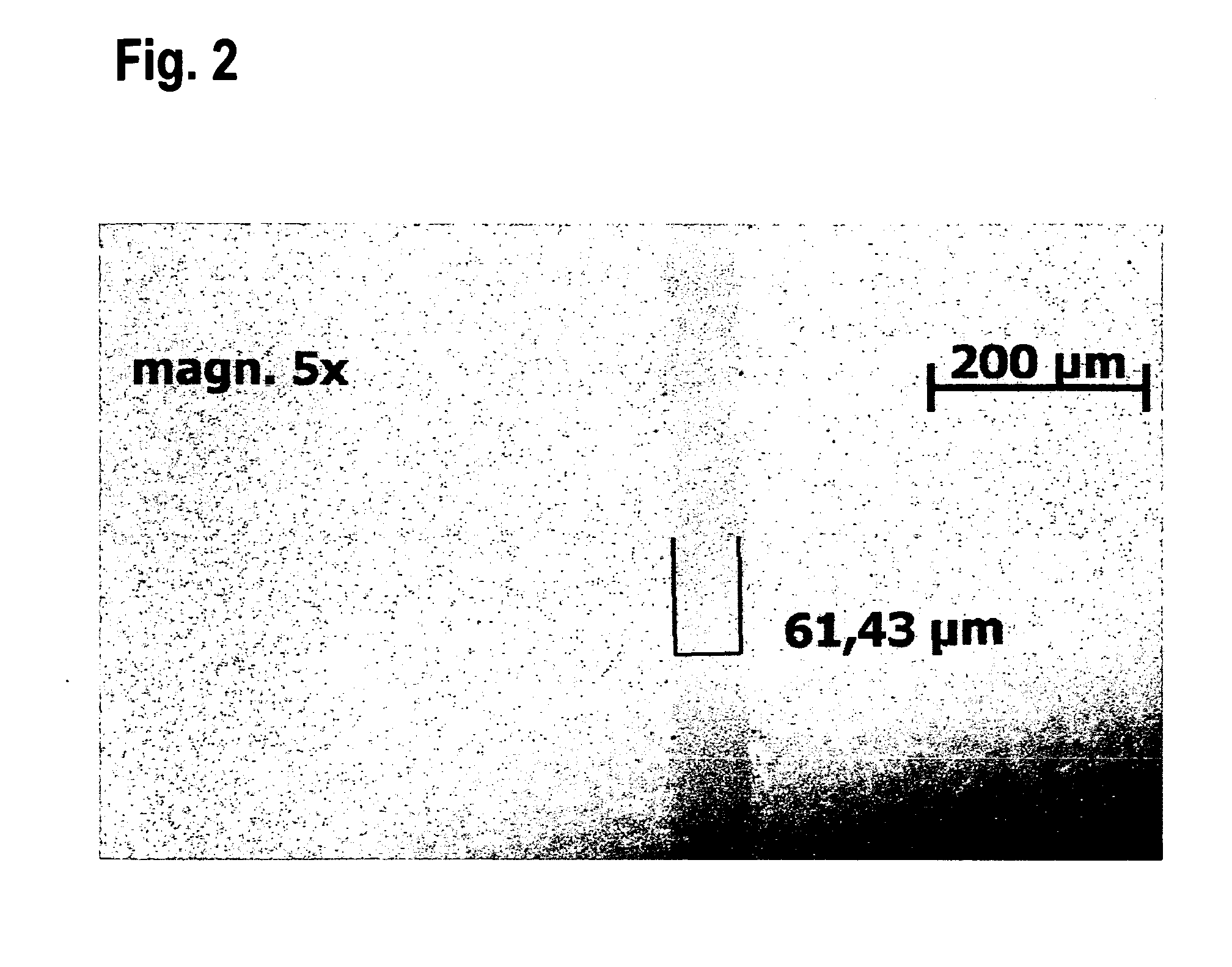
[0142]FIG. 1 shows the measured etching profile achieved with a composition according to example 1 and where a AgNW comprising polymer layer is etched at room temperature for 1 minute.

example 2

[0143]30 g Ethylenglycol

[0144]29 g Polycarbonat

[0145]72 g Ameisensaure (100%)

[0146]30 g DI Water

[0147]8 g Ammoniumhydrogendifluorid

[0148]8 g Polyvinylpyrollidone

[0149]75 g Vestosint 2070

example 3

[0150]33 g H3PO4

[0151]36 g 1-Methyl-2-pyrrolidone

[0152]13 g DI Water

[0153]8 g Polyvinylpyrollidone

[0154]3 g Graphite

[0155]The etching composition is mixed as described above. The result is a printable etching composition.


PUM

PropertyMeasurementUnit
temperatureaaaaaaaaaa
diameteraaaaaaaaaa
diameteraaaaaaaaaa

Abstract

The present invention refers to a method for selectively structuring of a polymer matrix comprising AgNW (silver nano wires) or CNTs (carbon nano tubes) or comprising mixtures of AgNW and CNTs on a flexible plastic substructure or solid glass sheet. The method also includes a suitable etching composition, which allows to proceed the method in a mass production.

Description

FIELD OF THE INVENTION[0001]The present invention refers to a method for a selective structuring of a polymer matrix comprising AgNW (silver nano wires) on a flexible plastic substructure or glass sheet. The method also includes a suitable etching composition for carrying the method out in the mass production.BACKGROUND OF THE INVENTION / STATE OF THE ART[0002]Transparent conductive films are very important for many electronic devices and components. They are mostly used for electrode applications in devices such as liquid crystals, flat panels or plasma displays, touch panels, organic light emitting diodes (OLED) and solar cells. Such films especially are used for thin film cells, organic polymer cells (OPC) and dye-sensitized solar cells.[0003]Transparent conductive film materials are usually made from doped metal oxides, most commonly indium tin oxide (ITO). However ITO has a number of drawbacks and is unlikely to be the material of choice in future optoelectronic devices.[0004]T...

Claims


Application Information

Patent Timeline
Patent Type & Authority Applications(United States)
IPC IPC(8): H01L51/00
CPCH01L51/0017C09K13/06C09K13/08C23F1/00C23F1/02C23F1/30H01B1/22H01L31/1888H01L33/42H10K71/236H10K71/621H10K10/82H10K50/826H10K50/828H10K2102/331Y02E10/50H10K71/231
Inventor STOCKUM, WERNERDOLL, OLIVERKOEHLER, INGOMATUSCHEK, CHRISTIAN
Owner MERCK PATENT GMBH
Why Eureka
Try Eureka