Single crystal CVD synthetic diamond material

a single crystal, synthetic diamond technology, applied in the direction of synthetic resin layered products, crystal growth process, polycrystalline material growth, etc., can solve the problem of difficult to even approach the level of perfection, all diamond materials contain a significant number of defects, and the thermodynamic perfection of diamond lattice is impossible to achieve. , to achieve the effect of good optical quality and low crystallographic defects

Active Publication Date: 2014-11-13
ELEMENT SIX LTD
View PDF5 Cites 64 Cited by
  • Summary
  • Abstract
  • Description
  • Claims
  • Application Information

AI Technical Summary

Benefits of technology

[0060]The single crystal CVD synthetic diamond material preferably also has low concentrations of impurities (other than nitrogen). For example, the material may have a concentration of silicon equal to or less than 1×10¹⁵ atoms cm−3. The material also preferably is fabricated to have low crystallographic defects. For example, the material may

Problems solved by technology

Such a theoretically perfect diamond lattice is thermodynamically impossible to attain.
In reality, it is practically difficult to even approach a level of perfection which would be possible to achieve in theory when taking into account thermodynamic considerations.
As such, it should be apparent that all diamond materials contain a significant number of defects.
Such defects may come in the form of impurities.
Additionally, defects within diamond materials also include crystallographic deviations from the perfect diamond lattice structure in the form of point defects such as vacancies and interstitials and extended defects such as various forms of dislocation defects.
Defects within diamond materials significantly alter the properties of the materials.
Furthermore, the nature of the substrate material and the growth conditions can affect the type and distribution of defects incorporated into the CVD synthetic diamond material during growth.
However, in such applications impurities can interact with quantum spin defects within the diamond lattice structure reducing their decoherence time and thus reducing their sensitivity and/or reducing the time during which quantum processing applications can be performed.
However for several applications, HPHT-grown diamond possesses additional qualities that are detrimental.
Growth tends to be highly non-uniform with a higher defect impurity (nitrogen as well as trace metals) in some sectors compared to others, and hence HPHT-grown diamond commonly exhibits colour zoning in both its as-grown and treated states.
These metal inclusions can strongly affect the mechanical properties of the material produced.
Nitrogen is one of the most important dopants in CVD diamond material synthesis as it has been found that providing nitrogen in the CVD process gas increases the growth rate of the material and can also affect the formation of crystallographic defects such as dislocations.
One problem with the aforementioned single layer structure is that the

Method used


Image

  • Single crystal CVD synthetic diamond material
  • Single crystal CVD synthetic diamond material
  • Single crystal CVD synthetic diamond material

Examples


examples

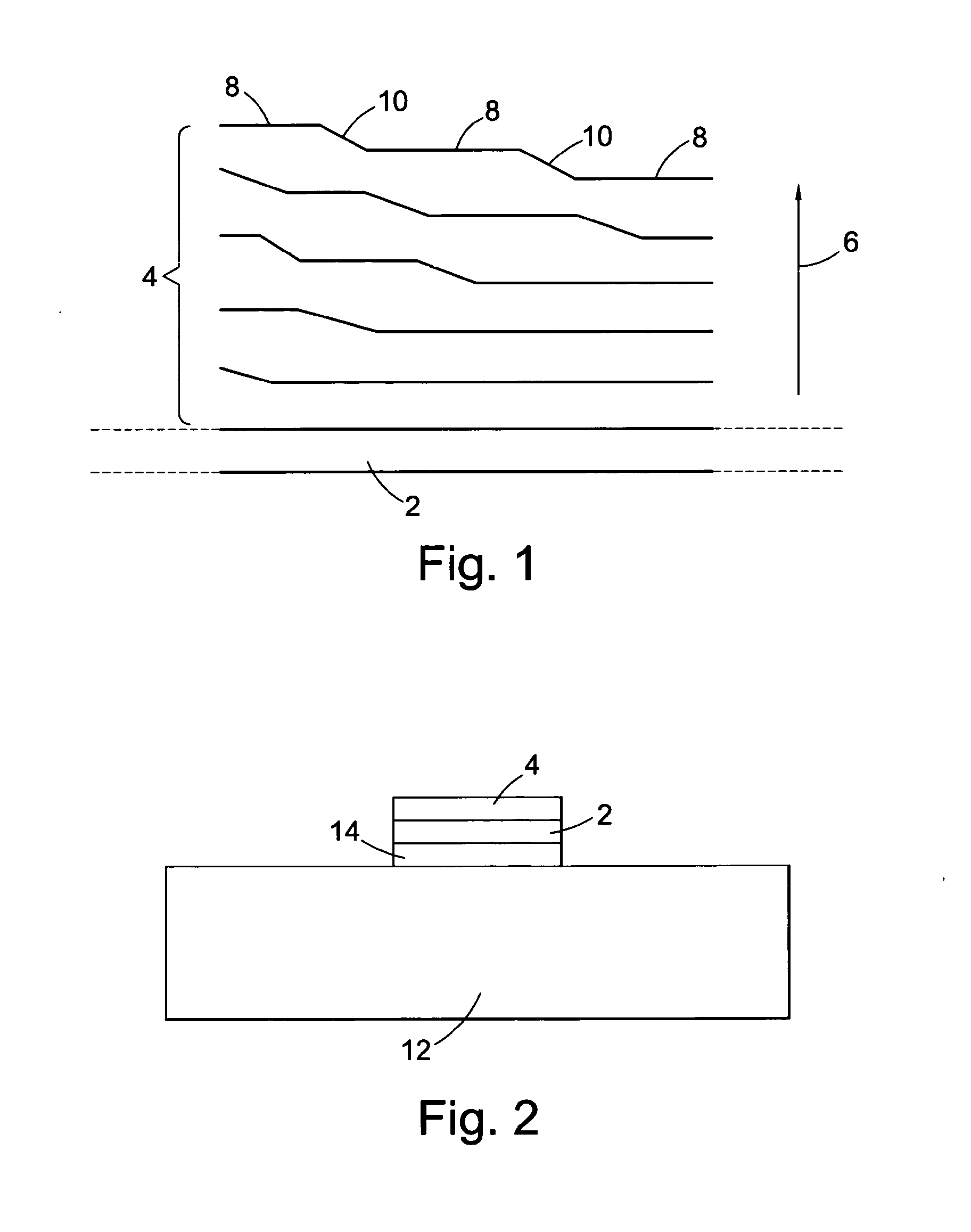
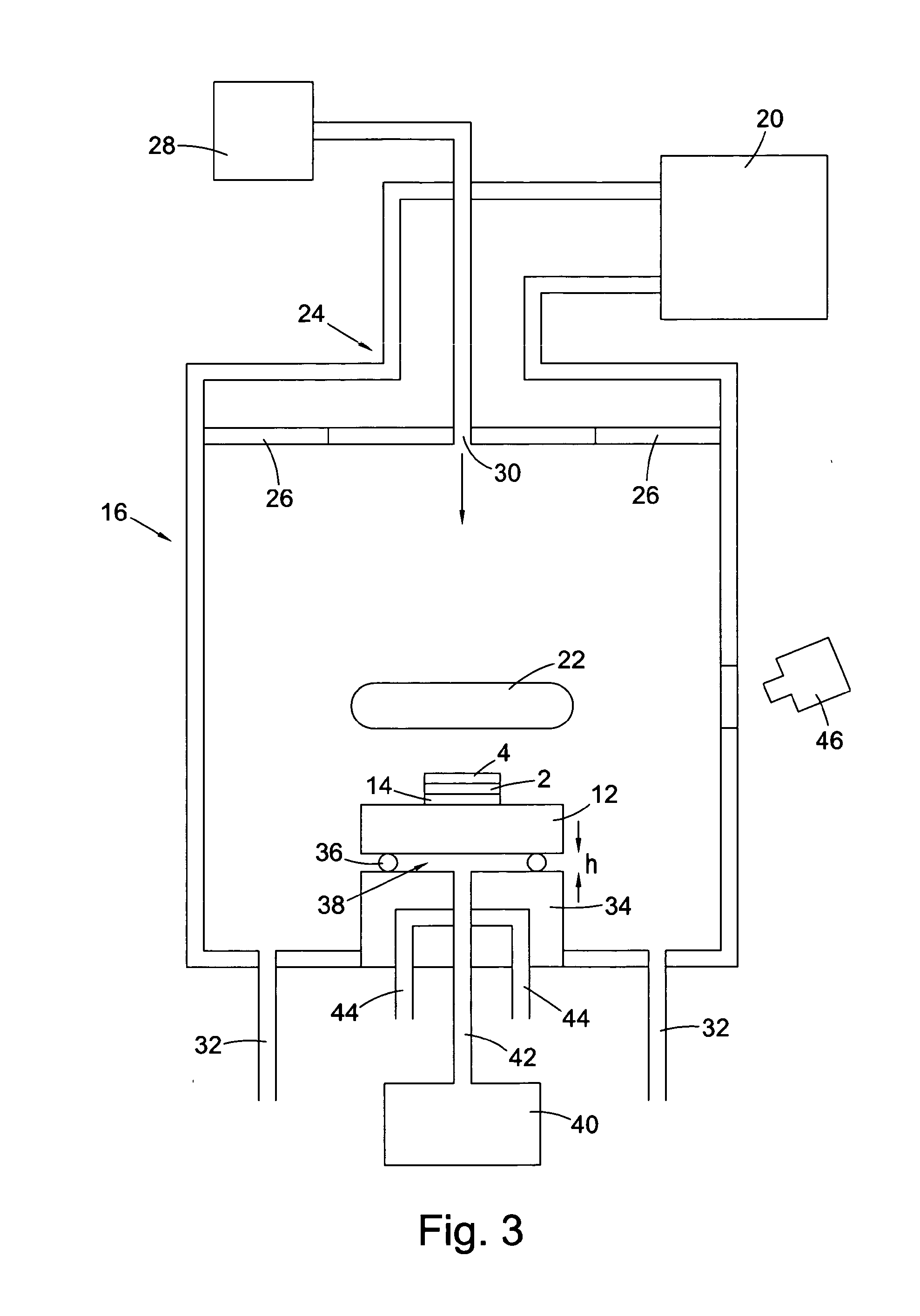
[0175]Utilizing the previously described CVD reactor and substrate configuration, single crystal CVD diamond material has been grown under high nitrogen / high substrate temperature conditions using various concentration of oxygen containing source gas and various concentrations of carbon source gas in the CVD synthesis atmosphere.

[0176]FIG. 4(a) is a DiamondView™ image of a single crystal CVD synthetic diamond material grown under high nitrogen / high substrate temperature conditions showing clearly visible striations. In this example the CVD synthesis atmosphere was formed using the following gas flow rate: 3000 sccm H2; 0 sccm CO2; 165 sccm CH4; and 4.0 sccm pure N2 (1254 ppm). These flow rates correspond to the following atomic concentrations: 97.5% H, 2.4% C; 0% 0; and 0.1% N.

[0177]In contrast, FIG. 4(b) is a DiamondView™ image of a single crystal CVD synthetic diamond material grown under high nitrogen / high substrate temperature / oxygen conditions showing substantially no visible s...


PUM

PropertyMeasurementUnit
Temperatureaaaaaaaaaa
Lengthaaaaaaaaaa
Lengthaaaaaaaaaa

Abstract

A single crystal CVD synthetic diamond material comprising: a total as-grown nitrogen concentration equal to or greater than 5 ppm, and a uniform distribution of defects, wherein said uniform distribution of defects is defined by one or more of the following characteristics: (i) the total nitrogen concentration, when mapped by secondary ion mass spectrometry (SIMS) over an area equal to or greater than 50×50 μm using an analysis area of 10 μm or less, possesses a point-to-point variation of less than 30% of an average total nitrogen concentration value, or when mapped by SIMS over an area equal to or greater than 200×200 μm using an analysis area of 60 μm or less, possesses a point-to-point variation of less than 30% of an average total nitrogen concentration value; (ii) an as-grown nitrogen-vacancy defect (NV) concentration equal to or greater than 50 ppb as measured using 77K UV-visible absorption measurements, wherein the nitrogen-vacancy defects are uniformly distributed through the synthetic single crystal CVD diamond material such that, when excited using a 514 nm laser excitation source of spot size equal to or less than 10 μm at room temperature using a 50 mW 46 continuous wave laser, and mapped over an area equal to or greater than 50×50 μm with a data interval less than 10 μm there is a low point-to-point variation wherein the intensity area ratio of nitrogen vacancy photoluminescence peaks between regions of high photoluminescent intensity and regions of low photolominescent intensity is <2× for either the 575 nm photoluminescent peak (NV0) or the 637 nm photoluminescent peak (NV); (iii) a variation in Raman intensity such that, when excited using a 514 nm laser excitation source (resulting in a Raman peak at 552.4 nm) of spot size equal to or less than 10 μm at room temperature using a 50 mW continuous wave laser, and mapped over an area equal to or greater than 50×50 μm with a data interval less than 10 μm, there is a low point-to-point variation wherein the ratio of Raman peak areas between regions of low Raman intensity and high Raman intensity is <1.25×; (iv) an as-grown nitrogen-vacancy defect (NV) concentration equal to or greater than 50 ppb as measured using 77K UV-visible absorption measurements, wherein, when excited using a 514 nm excitation source of spot size equal to or less than 10 μm at 77K using a 50 mW continuous wave laser, gives an intensity at 575 nm corresponding to NV0 greater than 120 times a Raman intensity at 552.4 nm, and/or an intensity at 637 nm corresponding to NV greater than 200 times the Raman intensity at 552.4 nm; (v) a single substitutional nitrogen defect (Ns) concentration equal to or greater than 5 ppm, wherein the single substitutional nitrogen defects are uniformly distributed through the synthetic single crystal CVD diamond material such that by using a 1344 cm−1 infrared absorption feature and sampling an area greater than an area of 0.5 mm2, the variation is lower than 80%, as deduced by dividing the standard deviation by the mean value; (vi) a variation in red luminescence intensity, as defined by a standard deviation divided by a mean value, is less than 15%; (vii) a mean standard deviation in neutral single substitutional nitrogen concentration of less than 80%; and (viii) a colour intensity as measured using a histogram from a microscopy image with a mean gray value of greater than 50, wherein the colour intensity is uniform through the single crystal CVD synthetic diamond material such that the variation in gray colour, as characterised by the gray value standard deviation divided by the gray value mean, is less than 40%.

Description

FIELD OF INVENTION[0001]Embodiments of the present invention relate to single crystal CVD (chemical vapour deposited) synthetic diamond material and methods of making the same.BACKGROUND OF INVENTION[0002]By way of background, a short introduction to diamond materials science is presented here in order to set the context for the present invention.[0003]Diamond materials are based on a theoretically perfect diamond lattice. The properties that would be exhibited by this theoretically perfect lattice are well understood. For example, such a theoretically perfect diamond lattice would exhibit extremely high thermal conductivity, low electrical conductivity (very wide band gap intrinsic semi-conductor with no significant charge carriers but with high charge carrier mobility if charge carriers are introduced into the lattice structure), extremely low thermal expansion coefficient, no significant optical birefringence, and low optical absorption (no significant absorption in the visible s...

Claims


Application Information

Patent Timeline
IPC IPC(8): C30B29/04
CPCC30B29/04C30B25/10C30B25/16C30B25/20C01B32/25C23C16/27C30B25/02C30B21/04C30B21/02
Inventor DHILLON, HARPREET KAURTWITCHEN, DANIEL JAMESKHAN, RIZWAN UDDIN AHMAD
Owner ELEMENT SIX LTD
Why Eureka
Try Eureka