

Semiconductor device and method for driving the same
a technology of semiconductor devices and driving methods, which is applied in semiconductor devices, digital storage, instruments, etc., can solve the problems of leakage current through gate insulating films, semiconductor devices do not benefit from the improvement of driving capability, and the charge retention characteristics of nodes deteriorate, so as to achieve excellent charge retention characteristics of nodes and fast data reading
- Summary
- Abstract
- Description
- Claims
- Application Information
AI Technical Summary
Benefits of technology
Problems solved by technology
Method used
Image

Examples
embodiment 1
[0049]In this embodiment, a circuit structure and operation of a semiconductor device will be described.
[0050]Note that a semiconductor device refers to a device including a semiconductor element. The semiconductor device includes a driver circuit for driving a circuit including a semiconductor element, for example. Note that the semiconductor device may include a driver circuit, a power supply circuit, or the like provided over another substrate, in addition to a memory cell.
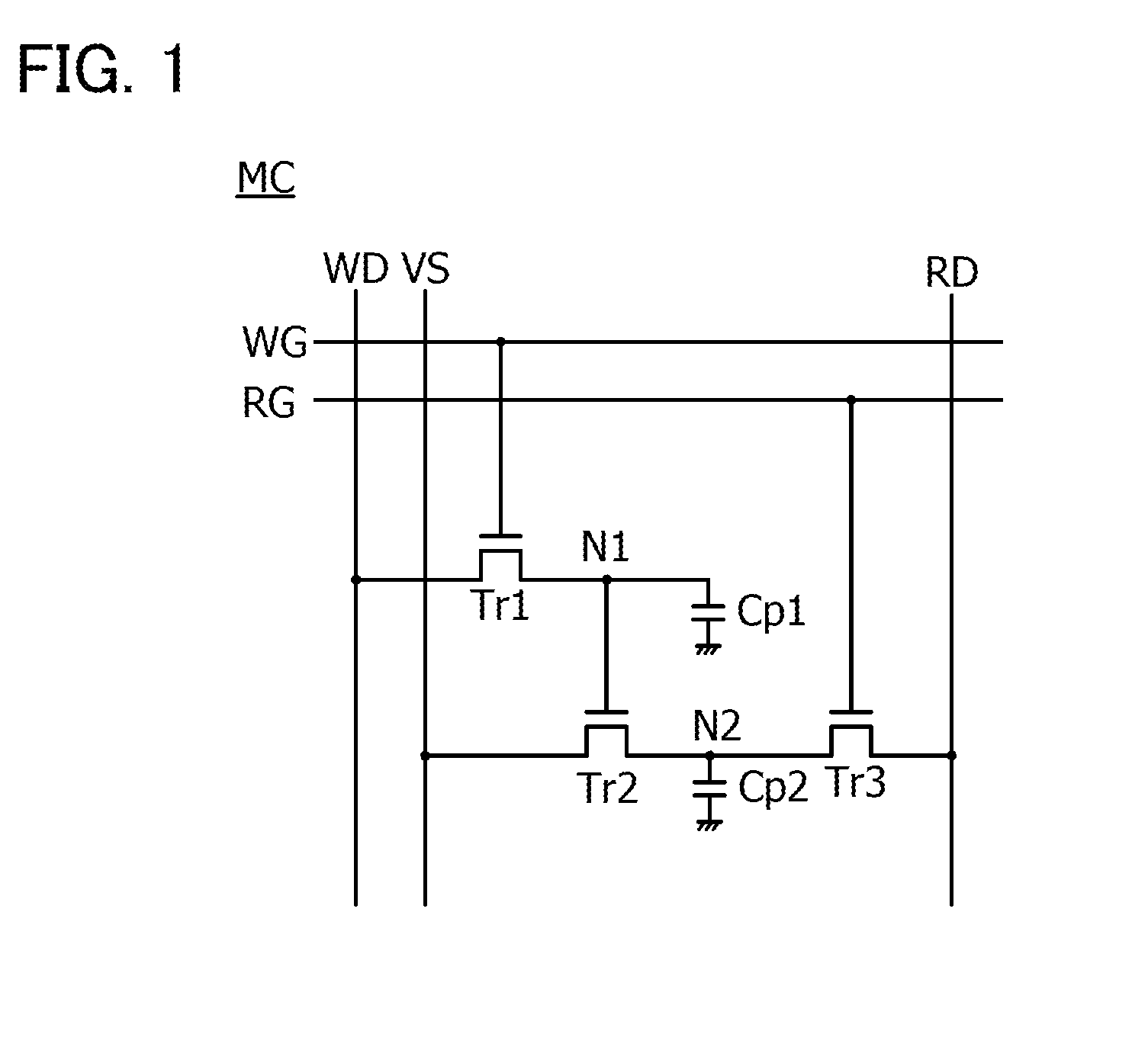
[0051]FIG. 1 is a circuit diagram illustrating an example of a memory cell MC included in a semiconductor device. In an actual semiconductor device, memory cells MC are arranged in a matrix.
[0052]First, components included in the memory cell MC will be described.
[0053]The memory cell MC illustrated in FIG. 1 includes a transistor Tr1, a transistor Tr2, a transistor Tr3, a capacitor Cp1, and a capacitor Cp2. Note that the transistors Tr1 to Tr3 are n-channel transistors in FIG. 1. In FIG. 1, a circuit portion co...
embodiment 2
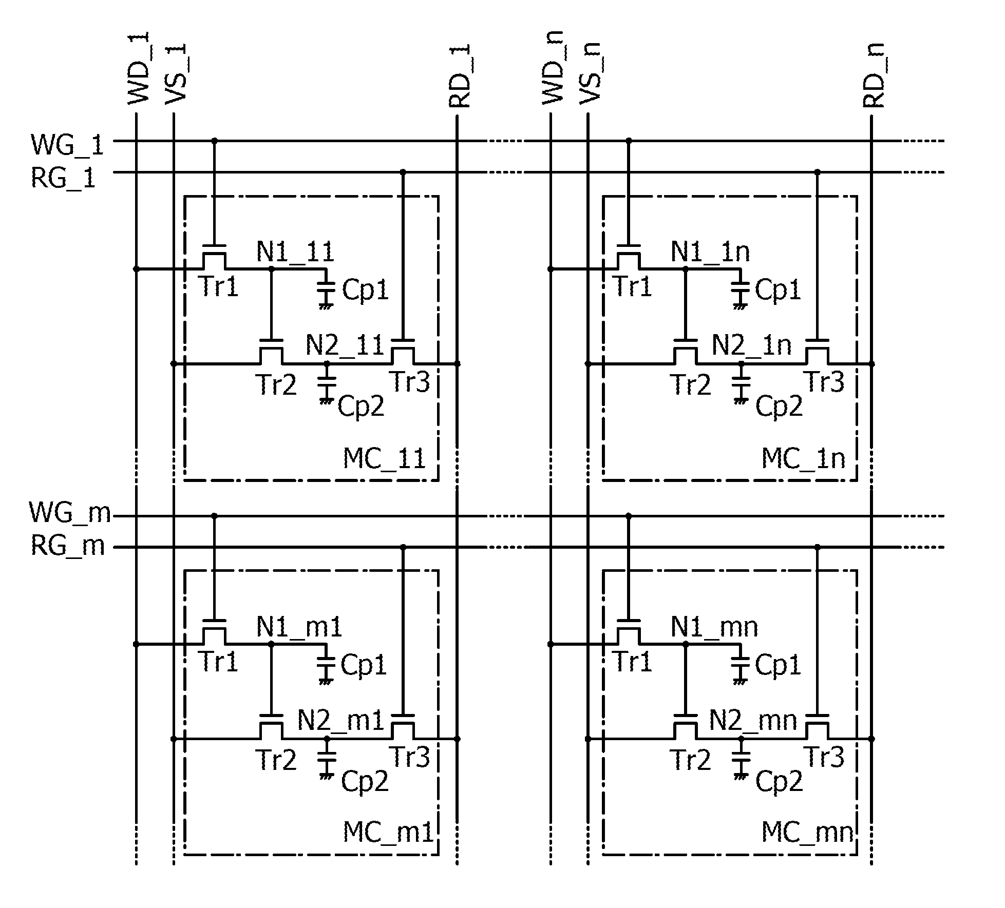
[0149]Referring to FIGS. 8 to 12, this embodiment will show an example of a semiconductor device including a matrix of the memory cells described in Embodiment 1.
[0150]FIG. 8 is a block diagram illustrating a structure example of a semiconductor device including the memory cells MC arranged in a matrix in FIG. 4.
[0151]A semiconductor device 200 illustrated in FIG. 8 includes a memory cell array 201 in which the memory cells MC_11 to MC_mn described using FIG. 4 in Embodiment 1 are arranged in a matrix, a row driver 202, a column driver 203, and a read driver 204. FIG. 8 also illustrates wirings connected to the memory cell MC_11 in the first row and the first column, the memory cell MC_1n in the first row and the n-th column, the memory cell MC_m1 in the m-th row and the first column, and the memory cell MC_mn in the m-th row and the n-th column, specifically the write selection line WG_1, the read selection line RG_1, the write selection line WG_m, the read selection line RG_m, the...
embodiment 3
[0172]This embodiment will explain an oxide semiconductor layer that can be used as a semiconductor layer including a channel formation region of the transistor with low off-state current described in the foregoing embodiments.
[0173]An oxide semiconductor used for the semiconductor layer including a channel formation region of the transistor preferably contains at least indium (In) or zinc (Zn). In particular, the oxide semiconductor preferably contains both In and Zn. The oxide semiconductor preferably contains a stabilizer for strongly bonding oxygen, in addition to In and Zn. The oxide semiconductor preferably contains at least one of gallium (Ga), tin (Sn), zirconium (Zr), hafnium (Hf), and aluminum (Al) as the stabilizer.
[0174]As another stabilizer, the oxide semiconductor may contain one or more kinds of lanthanoid such as lanthanum (La), cerium (Ce), praseodymium (Pr), neodymium (Nd), samarium (Sm), europium (Eu), gadolinium (Gd), terbium (Tb), dysprosium (Dy), holmium (Ho), ...
PUM
 Abstract
Description
Claims
Application Information