Oxide for semiconductor layer in thin film transistor, thin film transistor, display device, and sputtering target

Active Publication Date: 2015-03-19
KOBE STEEL LTD
View PDF2 Cites 11 Cited by
  • Summary
  • Abstract
  • Description
  • Claims
  • Application Information

AI Technical Summary

Benefits of technology

[0029]The present invention can provide an oxide to be used as a semiconductor layer in a thin film transistor having high mobility, switching characteristics, stress resistance shown by a small variation of threshold voltage before and after applying the light irradiation and the electrically negative biasing. In addition, the oxide is superior in terms of the durability in a wet etchant used for patterning a source-drain electrode. A display device of high reliability can be pr

Problems solved by technology

In addition, for example, when a liquid crystal display panel is driven or when a negative bias is applied to the gate electrode to turn on a pixel, the TFT is irradiated with light leaked out from the liquid crystal cell, and this light gives stress to the TFT to cause deterioration in the characteristics.
Indeed, when a thin film transistor is used, a variation of switching characteristics due to stress by voltage application causes deterioration of reliability in a display devices itself.
Such a shift of threshold voltage of the TFT deteriorates the reliability of display devices such as a liquid crystal display and an organic EL display.
The oxide semiconductor, however, also shows high solubility into inorganic acid-based wet etchants, and is extremely easily etched b

Method used


Image

  • Oxide for semiconductor layer in thin film transistor, thin film transistor, display device, and sputtering target
  • Oxide for semiconductor layer in thin film transistor, thin film transistor, display device, and sputtering target
  • Oxide for semiconductor layer in thin film transistor, thin film transistor, display device, and sputtering target

Examples


Example

Example 1

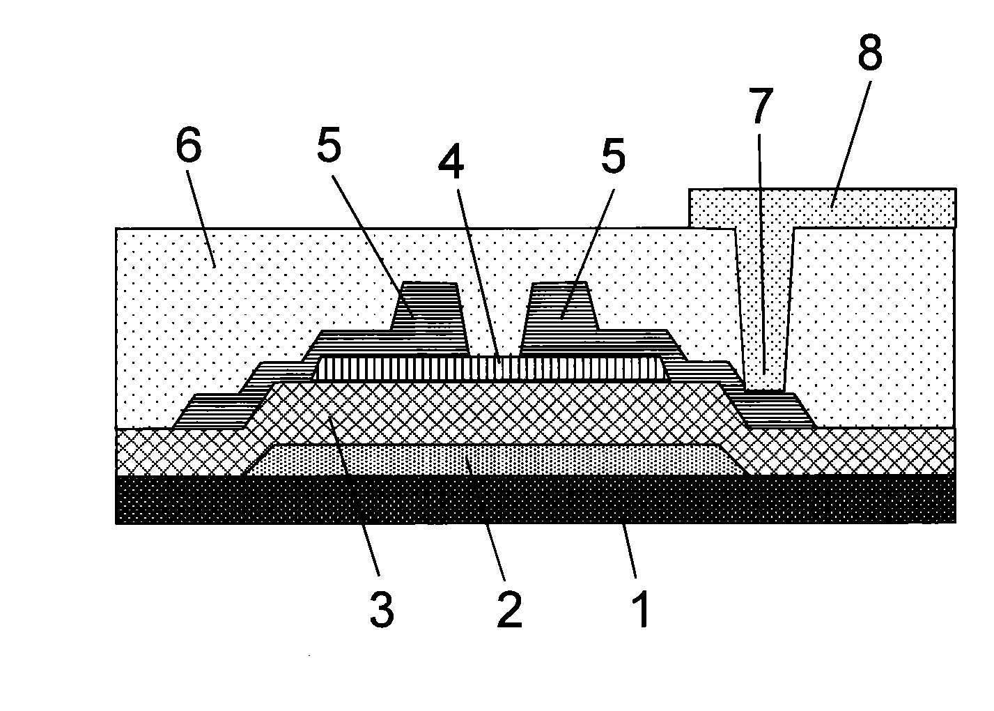
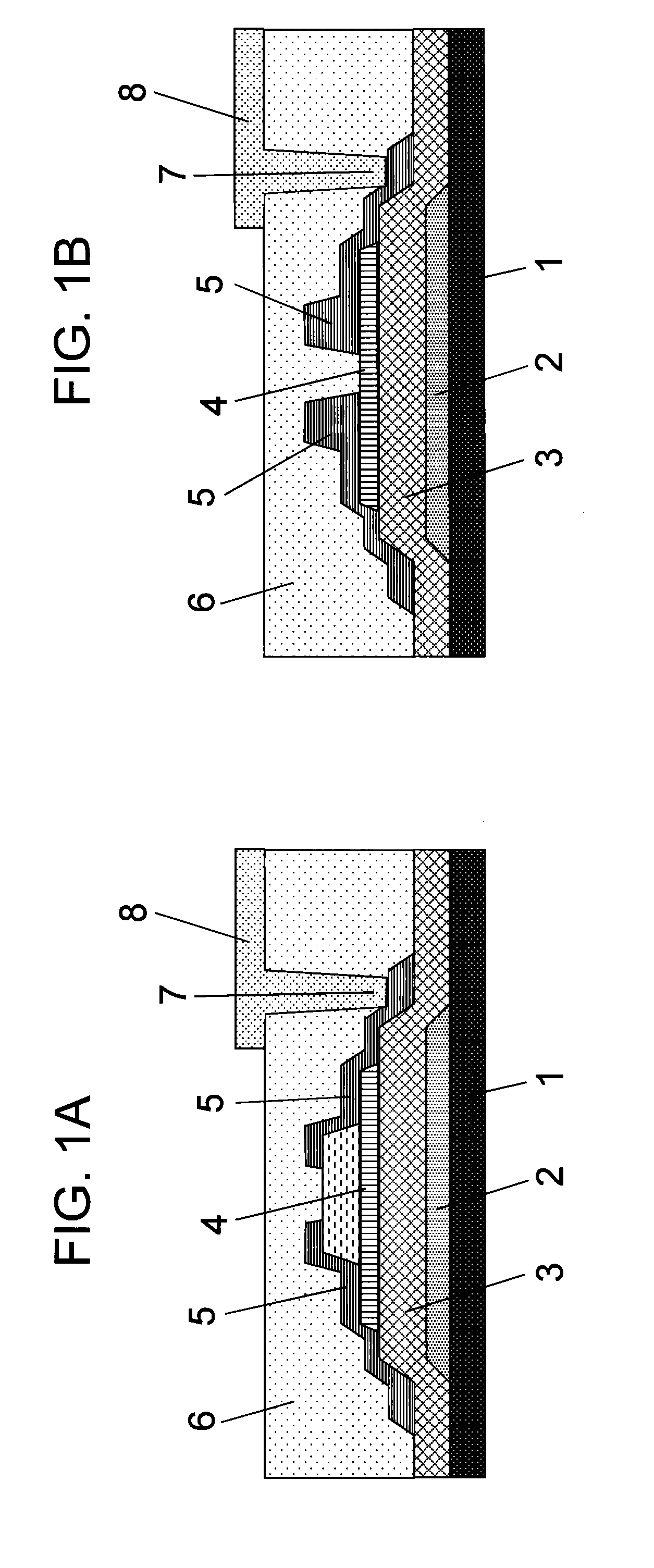
[0108]According to the method described above, TFTs having a structure depicted in FIG. 1B were fabricated. After forming a passivation film (insulating film) 6, their TFT characteristics were evaluated. In the present Example, an etch stopper layer 9 as illustrated in FIG. 1A was not formed.

[0109]First, a Mo thin film of 100 nm in thickness as a gate electrode 2 and SiO2 film of 200 nm in thickness as a gate insulating film 3 were successively deposited on a glass substrate 1 (“EAGLE 2000” available from Corning Inc, having a diameter of 100 mm and a thickness of 0.7 mm). The gate electrode 2 was deposited using a pure Mo sputtering target by a DC sputtering method under the conditions: deposition temperature, room temperature; sputtering power density, 3.8 W / cm2; carrier gas, Ar; gas pressure, 2 mTorr; Ar gas flow rate, 20 sccm. Further, the gate insulating film 3 was formed by a plasma CVD method under the conditions: carrier gas, a mixed gas of SiH4 and N2O; plasma powe...

Example

Example 2

[0177]In this Example, a relationship between [Sn], the content of Sn relative to the total content of all the metal elements and the wet etching rate was investigated for IZGTO. A wet etching test was carried out in a similar manner to Example 1.

[0178]Specifically, oxide thin films having various Sn ratios to all the metals constituting IGZTO while keeping the chemical composition ratio of metal elements other than Sn constant (In:Ga:Zn=20:30:50 in atomic %) were prepared. The thin films were deposited by sputtering method using sputtering targets containing different ratios of Sn.

[0179]The results are shown in FIG. 5. The abscissa of FIG. 5 is the content of Sn relative to the total content of all the metal elements [Sn], and the ordinate represents the wet etching rate.

[0180]As depicted in FIG. 5, the wet etching rate showed a rapid increase when the content of Sn was smaller than 5%. On the other hand, when the content of Sn is larger than or equal to 5%, the wet etchin...


PUM

PropertyMeasurementUnit
Densityaaaaaaaaaa
Electrical resistanceaaaaaaaaaa
Electric potential / voltageaaaaaaaaaa

Abstract

Provided is an oxide semiconductor configured to be used in a thin film transistor having high field-effect mobility; a small shift in threshold voltages against light and bias stress; excellent stress resistance. The oxide semiconductor has also excellent resistance to a wet-etchant for patterning of a source-drain electrode. The oxide semiconductor comprises In, Zn, Ga, Sn and O, and satisfies the requirements represented by expressions (1) to (4) shown below, wherein [In], [Zn], [Ga], and [Sn] represent content (in atomic %) of each of the elements relative to the total content of all the metal elements other than oxygen in the oxide.
(1.67×[Zn]+1.67×[Ga])≧100   (1)
{([Zn]/0.95)+([Sn]/0.40)+([In]/0.4)}≧100   (2)
[In]≦40   (3)
[Sn]≧5   (4)

Description

FIELD OF TECHNOLOGY[0001]The present invention relates to an oxide for semiconductor layer in a thin film transistor (TFT) used in display devices such as liquid crystal displays and organic EL displays; a thin film transistor having the oxide; a display device having the thin film transistor; and a sputtering target used in deposition of the oxide.BACKGROUND ART[0002]As compared with widely used amorphous silicon (a-Si), amorphous (non-crystalline), oxide semiconductors have high carrier mobility (also called as field-effect mobility, which may hereinafter be referred to simply as “mobility”), wide optical band gaps, and film formability at low temperatures, and therefore, have highly been expected to be applied for next generation displays, which are required to have large sizes, high resolution, and high-speed drives; resin substrates having low heat resistance; and others.[0003]In the oxide semiconductors, amorphous oxide semiconductors consisting of indium, gallium, zinc and ox...

Claims


Application Information

Patent Timeline
IPC IPC(8): H01L29/786H01J37/34
CPCH01L29/7869H01J2237/332H01J37/3429C23C14/086C23C14/3414H01L21/02554H01L21/02565C23C14/08H10K59/1213
Inventor MORITA, SHINYAHIROSE, KENTAMIKI, AYAKUGIMIYA, TOSHIHIRO
Owner KOBE STEEL LTD
Why Eureka
Try Eureka