

Pattern forming method, actinic ray-sensitive or radiation-sensitive resin composition, resist film, method for manufacturing electronic device, and electronic device
a technology of resist film and resin composition, which is applied in the direction of photosensitive materials, instruments, photomechanical equipment, etc., can solve the problems of difficult to solve and affect the shape of the obtained pattern, and achieve the effects of good scalability, good scalability, and good scalability
- Summary
- Abstract
- Description
- Claims
- Application Information
AI Technical Summary
Benefits of technology
Problems solved by technology
Method used
Image


Examples
examples
[0382]Hereinafter, more detailed description will be given according to Examples of the invention, but the present invention is not limited to the following Examples.
synthesis example
Synthesis of Resin P-01
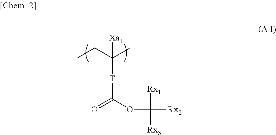
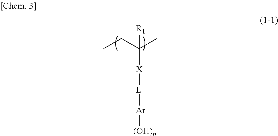
[0383]141.8 parts by mass of cyclohexanone were heated to 80° C. under a nitrogen stream. While stirring the solution, a mixed solution of 13.2 parts by mass of the monomer represented by the following structural formula A, 12.6 parts by mass of the monomer represented by the following structural formula B, 17.1 parts by mass of the monomer represented by the following structural formula C, 2.6 parts by mass of the monomer represented by the following structural formula D, 116.0 parts by mass of cyclohexanone, and 2.76 parts by mass of 2,2′-dimethyl azobisisobutyrate [V-601, manufactured by Wako Pure Chemical Industries (Ltd.)] was added dropwise over 4 hours. After the completion of the dropwise addition, stirring was further performed for two hours at 80° C. After cooling the reaction solution, 40.4 parts by mass of the resin (P-01) of the present invention were obtained by vacuum drying the solid which was obtained by re-precipitating and filtering in a lar...
PUM
| Property | Measurement | Unit |
|---|---|---|
| temperature | aaaaa | aaaaa |
| temperature | aaaaa | aaaaa |
| temperature | aaaaa | aaaaa |
Abstract
Description
Claims
Application Information