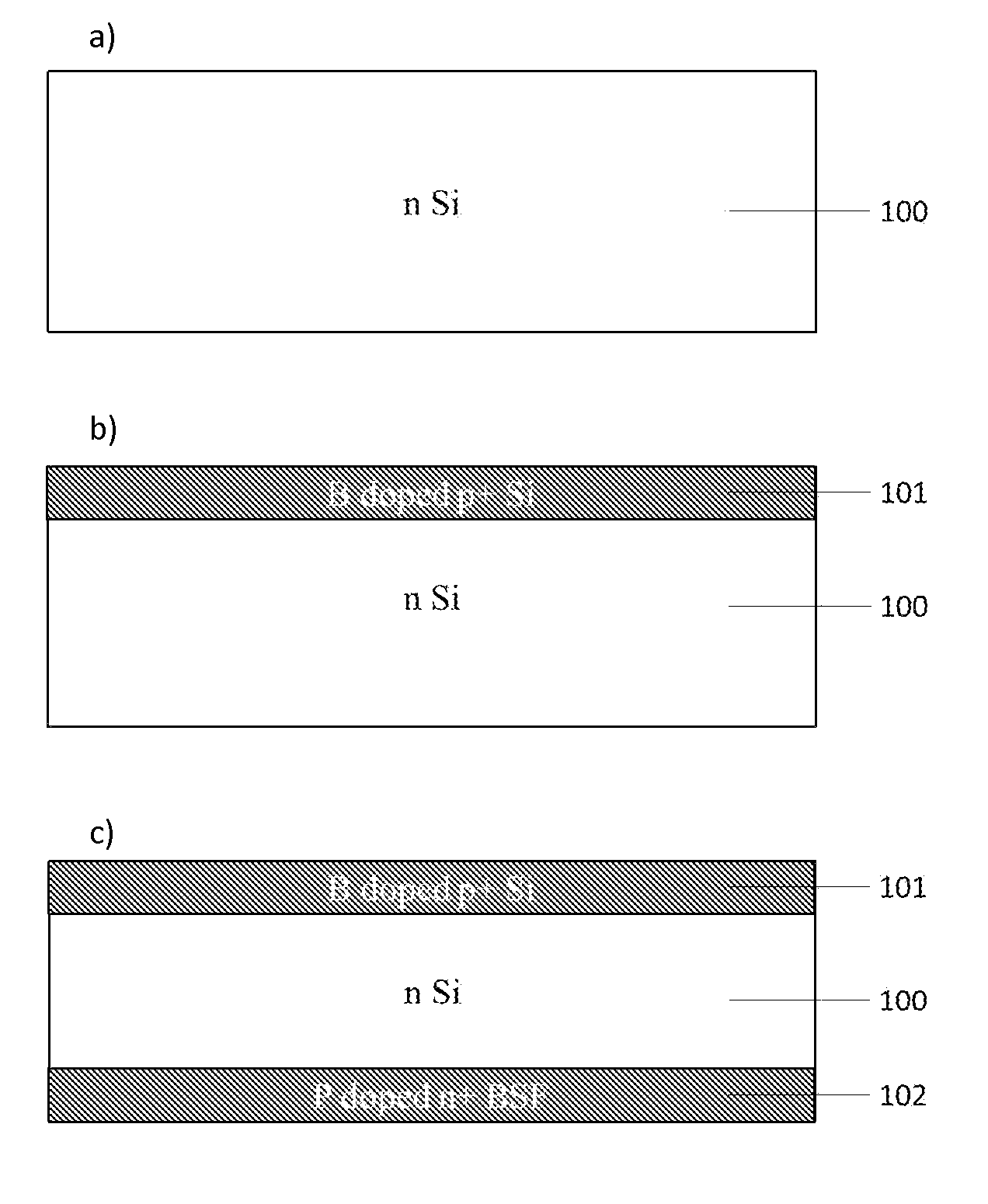
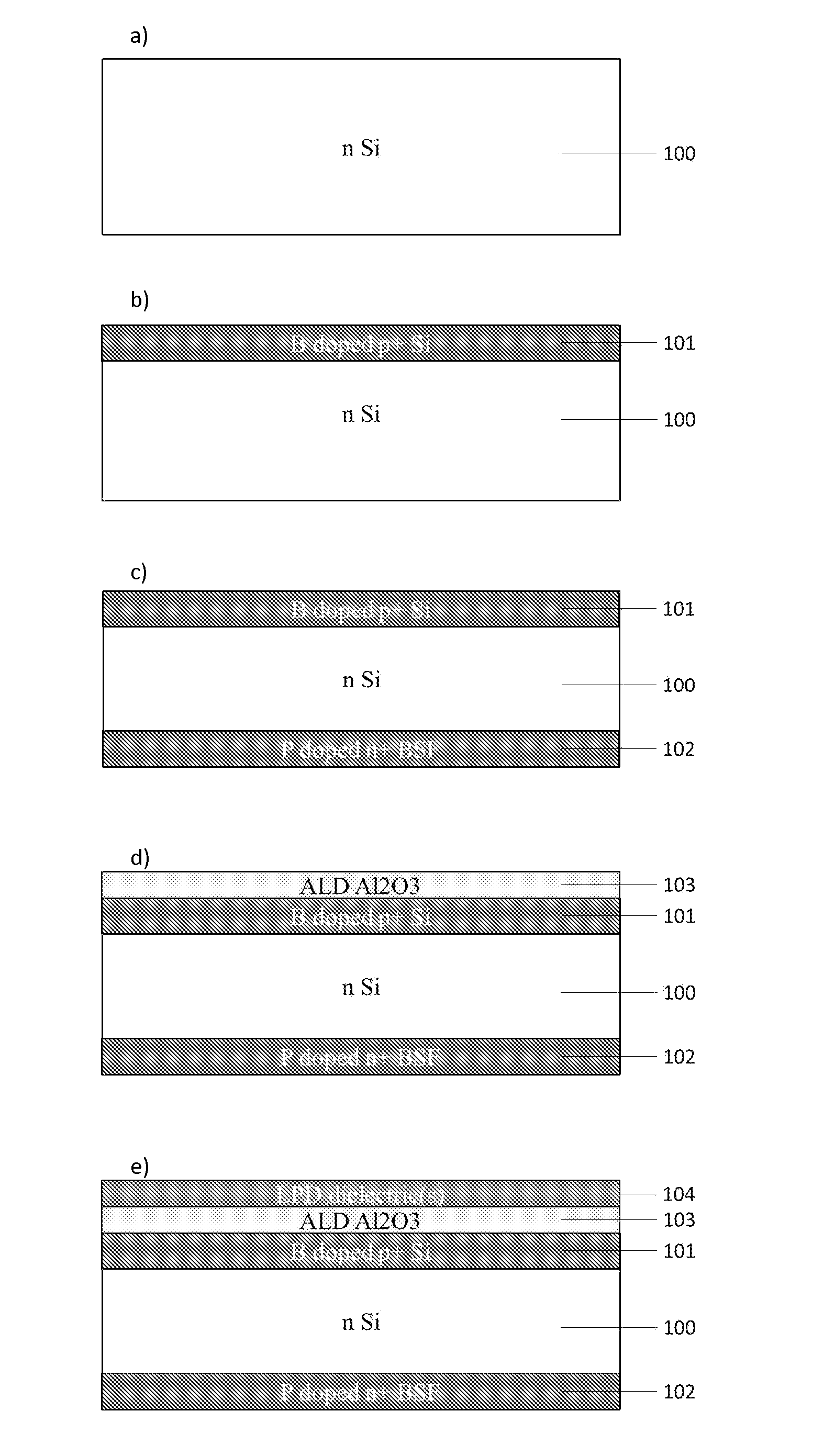
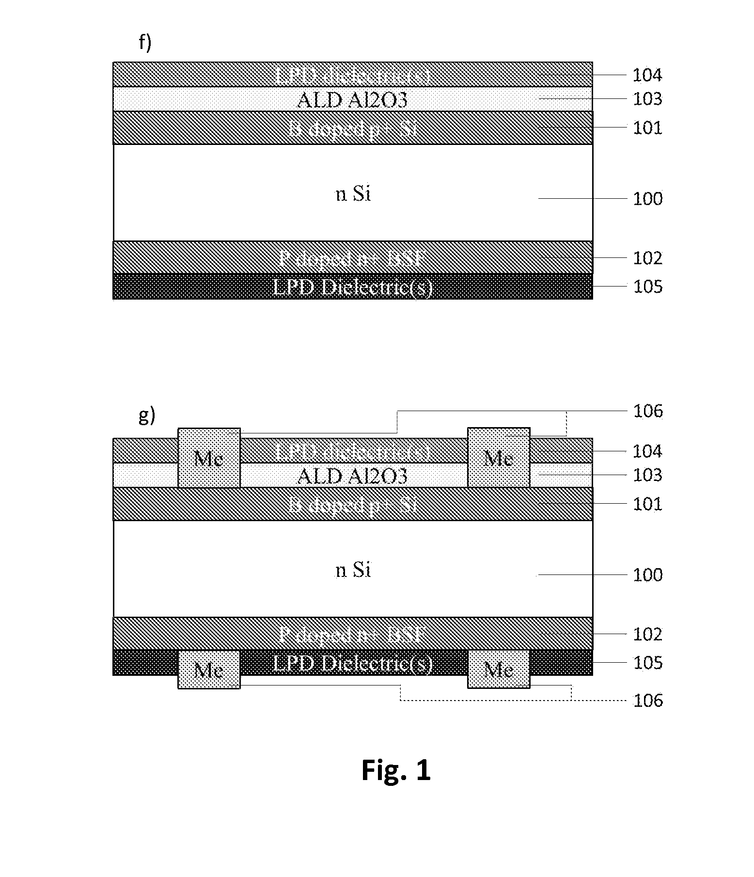
Method of modifying an n-type silicon substrate
a technology of silicon substrate and crystalline silicon, which is applied in the direction of photovoltaic energy generation, liquid/solution decomposition chemical coating, coating, etc., can solve the problems of relative high cost of manufacturing tools, consumable chemicals and gases, etc., and achieves the improvement of electrical or optical performance, low cost, and the effect of increasing the efficiency of current extraction
- Summary
- Abstract
- Description
- Claims
- Application Information
AI Technical Summary
Benefits of technology
Problems solved by technology
Method used
Image

Examples
example 1
[0096]Tetraethyl orthosilicate (28.00 g) and Triethoxysilane (42.00 g) and solvent (ethanol) were weighted into the 1 L flask and stirred for 30 minutes. 0.01 M HCl (2× equivalent) was added. Material was refluxed for one hour. Solvent exchange was done to propylene glycol propyl ether (PnP). A further condensation polymerization was carried out in presence of catalyst (triethylamine). After this trimethylmethoxysilane (0.02 g) was added and further solvent exchange done to propylene glycol propyl ether (PnP). Material was diluted to process formulation and filtrated with 0.1 μm filter to obtain process ready solution.
example 2
[0097]Tetraethyl orthosilicate (14.00 g) and Triethoxysilane (60.00 g) and solvent (2-propanol) were weighted into the 1 L flask and stirred for 30 minutes. 0.01 M HCl (0.6 equivalent) was added. Material was refluxed for one hour. Solvent exchange was done to propandiol-monobutyl ether (PNB). A further condensation polymerization was carried out in presence of catalyst (triethylamine). After this trimethylmethoxysilane (0.021 g) was added and further solvent exchange done to propylene glycol propyl ether (PnP). Material was diluted to process formulation and filtrated with 0.1 μm filter to obtain process ready solution.
example 3
[0098]Methyl-trimethoxysilane (15.00 g), 3-Glycidoxypropyl-trimethoxysilane (9.00 g) and Triethoxysilane (75.00 g) and solvent (2-propanol) were weighted into the 1 L flask and stirred for 30 minutes. 0.01 M HCl (1 equivalent) was added. Material was refluxed for one hour. Solvent exchange was done to propylene glycol propyl ether (PnP). A further condensation polymerization was carried out in presence of catalyst (triethylamine). After this trimethylethoxysilane (0.025 g) was added and further solvent exchange done to propylene glycol propyl ether (PnP). Material was diluted to process formulation and filtrated with 0.1 μm filter to obtain process ready solution.
PUM
| Property | Measurement | Unit |
|---|---|---|
| thicknesses | aaaaa | aaaaa |
| thickness | aaaaa | aaaaa |
| surface recombination velocity | aaaaa | aaaaa |
Abstract
Description
Claims
Application Information
 - Generate Ideas
- Intellectual Property
- Life Sciences
- Materials
- Tech Scout
- Unparalleled Data Quality
- Higher Quality Content
- 60% Fewer Hallucinations
Browse by: Latest US Patents, China's latest patents, Technical Efficacy Thesaurus, Application Domain, Technology Topic, Popular Technical Reports.
© 2025 PatSnap. All rights reserved.Legal|Privacy policy|Modern Slavery Act Transparency Statement|Sitemap|About US| Contact US: help@patsnap.com