Electroluminescence element

a technology of electroluminescence element and electroluminescence, which is applied in the direction of luminescent compositions, organic semiconductor devices, thermoelectric devices, etc., can solve the problems of high barrier properties of expensive barrier films, low performance of existing fluorescent light and white led, and inability to meet the requirements of further higher efficiency and prolonged lifetime, etc., to achieve excellent product quality, high light emission efficiency, and long lifetime

Inactive Publication Date: 2015-10-08
KONICA MINOLTA INC
View PDF4 Cites 34 Cited by
  • Summary
  • Abstract
  • Description
  • Claims
  • Application Information

AI Technical Summary

Benefits of technology

[0069]According to the present invention, an electroluminescence element having a high light emission efficiency and long lifetime, and further, an electroluminescence element having excellent productivity (calcination temperature, calcination time, and the like) on a plastic film can be provided.

Problems solved by technology

Also, while these new values are expected, performance to an existing fluorescent light and white LED is currently low, and technology for further higher efficiency and prolonged lifetime are required.
However, a phosphorescent organic EL element (OLED; Organic Light-Emitting Diode) is sensitive to oxygen and moisture, thus when being used as the flexible lighting as described above, an expensive barrier film having high barrier properties and treatment of step with low productivity (vacuum deposition, application process in an inert atmosphere, and the like) are required, thus it cannot be necessarily said as inexpensive and highly producible.
In such application process, an electroluminescence element on the plastic substrate cannot be produced by the simple application under atmospheric pressure as described above, and it has been a barrier to obtain an ideal electroluminescence element.
In addition, a metal oxide thin film generally has high surface roughness, and a dark spot caused by a leak is likely to occur, and has a problem also in the lifetime.
Yet, an electric field electroluminescence element using quantum dots, particularly, a host compound appropriate as a blue electroluminescence element has not been found so far, and still has a problem with regard to the lifetime.

Method used


Image

  • Electroluminescence element
  • Electroluminescence element
  • Electroluminescence element

Examples


example 1

Confirmation of Lamination Coatability of Compound of Present Invention

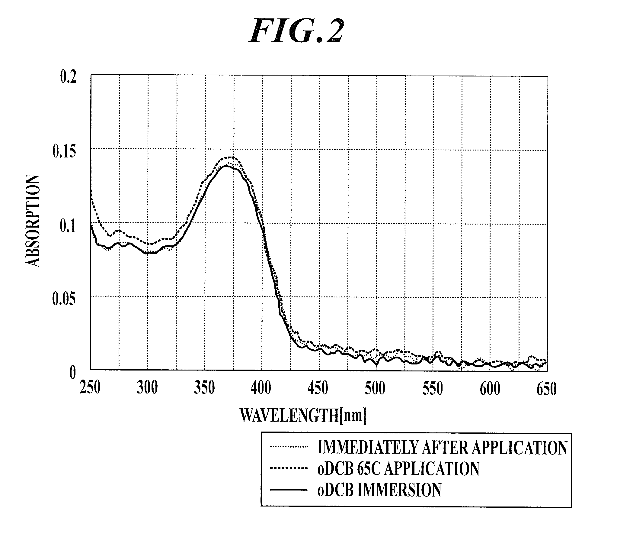
[0330]A quartz glass substrate was cleaned in order of ultrasonic cleaning with a surfactant and ultrapure water and ultrasonic cleaning with ultrapure water, then dried by blowing nitrogen, and finally subjected to UV ozone cleaning.

[0331]On the cleaned substrate, a solution was prepared by dissolving Exemplary Compound 15 in hexafluoroisopropanol so as to have a concentration of 0.1% by mass.

[0332]This solution was applied and dried on the quartz glass substrate using a blade coater controlled to a temperature of 65° C., so as to have a dry film thickness of about 20 nm. Thereafter, the dried film was heat-treated with a hot air at 100° C. for 2 minutes, to forma coating film of Exemplary Compound 15.

[0333]In FIG. 2, the spectrum of this coating film is a spectrum with a thin dotted-line (immediately after application). In addition, the spectrum of the film obtained by applying again only o-dichlorobenzene on ...

example 2

Preparation of Blue Light Emitting EL Element

(1) Preparation of Comparative Example Sample 1

(1.1) Preparation of Gas-Barrier Flexible Film

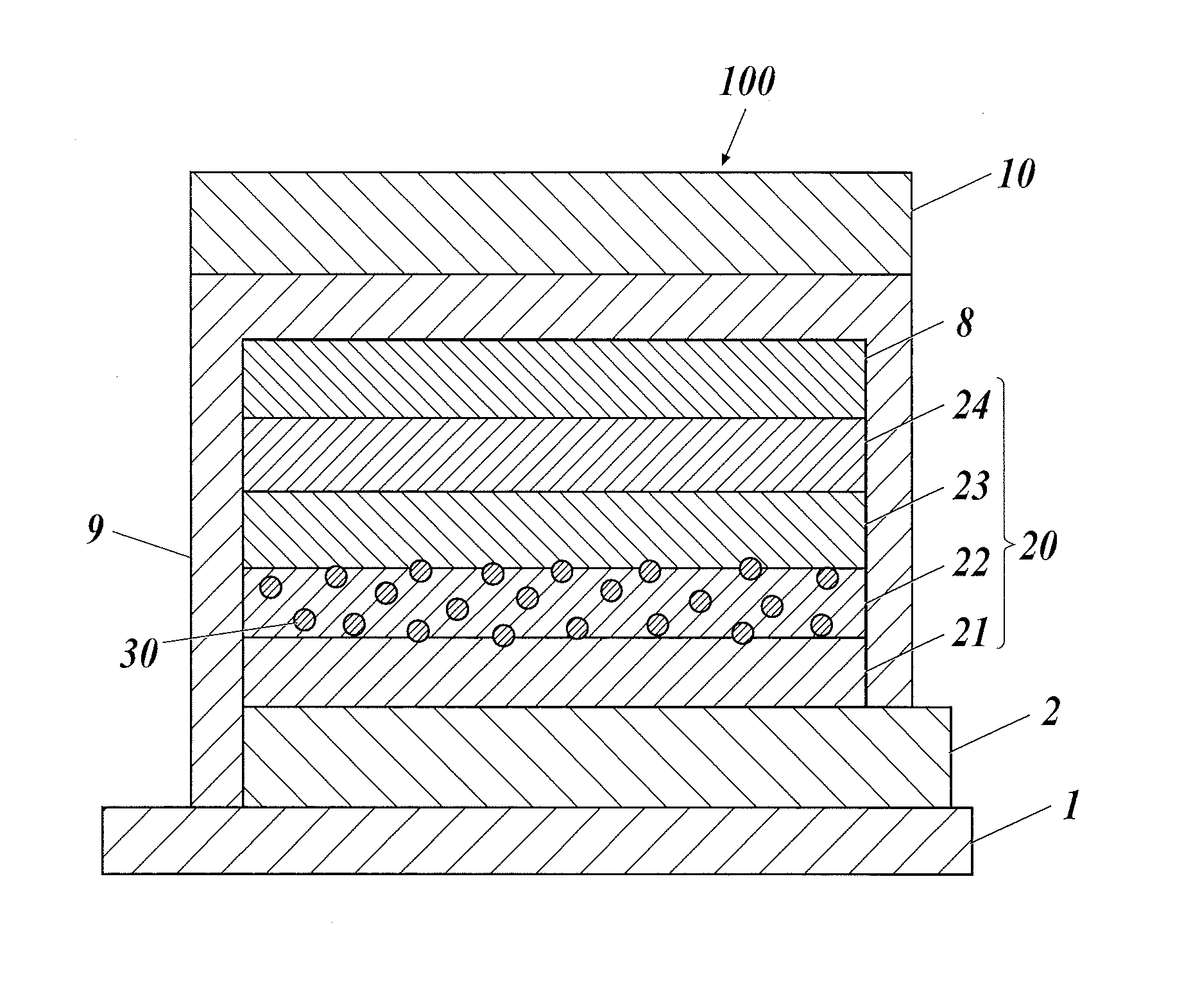
[0335]As a flexible film, a gas barrier film of an inorganic matter made of SiOx was formed successively on the flexible film, on the entire surface of the side in which a first electrode of a polyethylene naphthalate film (a film manufactured by Teijin DuPont Films Japan Limited, hereinafter abbreviated as PEN) was formed so as to have a thickness of 500 nm, using an atmospheric pressure plasma discharge treatment device comprising the constitution described in Japanese Patent Application Laid Open Publication No. 2004-68143, to prepare a gas barrier flexible film having an oxygen permeability of 10E-4 ml / m2 / day or less and a water vapor permeability of 10E-4 g / m2 / day or less.

(1.2) Formation of First Electrode

[0336]A film was formed with ITO (indium tin oxide) having a thickness of 120 nm on the prepared gas barrier flexible film by a sputtering ...

production example 1

Synthesis of Exemplary Compound 10

[0366]Exemplary Compound 10 was synthesized by the following reaction.

[0367]Compound B was synthesized with reference to Adv. Mater. 2007, 19, 2010. The weight average molecular weight of Compound B was 4400. 1.0 g of Compound B and 5.5 g of N,N,N′-trimethylethylenediamine (manufactured by Sigma-Aldrich Co. LLC.) were dissolved in a mixed solvent of 100 ml of tetrahydrofuran and 100 ml of N,N-dimethylformamide, and the solution was stirred at room temperature (25° C.) for 48 hours to carry out a reaction. After the completion of the reaction, the solvent was distilled off under reduced pressure, and the residue was further redeposited in water to obtain 1.0 g of Exemplary Compound 10 (yield 90%).


PUM

PropertyMeasurementUnit
thicknessaaaaaaaaaa
wavelengthaaaaaaaaaa
particle sizeaaaaaaaaaa

Abstract

Disclosed is an electroluminescence element, wherein at least a first electrode, a light-emitting layer, and a second electrode may be laminated on a substrate in said order. In said element, the light-emitting layer may contain quantum dots, and an intermediate layer formed from a polymer containing nitrogen atoms may be formed between the first electrode and the light-emitting layer.

Description

TECHNICAL FIELD[0001]The present invention relates to an electroluminescence element (EL element), and in more detail, an electroluminescence element having excellent light emission efficiency and emission lifetime.BACKGROUND ART[0002]In recent years, an organic electroluminescence element using an organic substance (hereinafter, appropriately abbreviated as “organic EL element” or “OLED; Organic Light-Emitting Diode”.) is promised as a use as a solid light emitting large-area full color display element that is lightweight, thin, high-efficient and inexpensive and a light source array, and the research and development is actively advanced.[0003]Particularly in a mobile body (cell phone, automobile, aircraft), a lighting that is thinner and lighter than conventional ones and hard to crack (lighting composed of a flexible substrate) is expected. Also, while these new values are expected, performance to an existing fluorescent light and white LED is currently low, and technology for fu...

Claims


Application Information

Patent Timeline
Patent Type & Authority Applications(United States)
IPC IPC(8): H01L51/00
CPCH01L51/0036H01L51/5044H01L51/0073H01L51/0039H01L51/004H01L51/502H01L51/5206H01L51/5096H01L51/5056H01L51/5088H01L51/5221H01L2251/301H01L2251/308H01L51/5278H01L51/5016H01L51/0085B82Y20/00C09K11/06H05B33/14H10K85/141H10K85/113H10K85/115H10K85/151H10K50/115H10K50/11H10K2101/10H10K50/15H10K85/342H10K85/6574H10K50/17H10K50/18H10K50/19H10K50/81H10K50/82H10K50/131H10K2102/00H10K2102/103
Inventor OKUBO, YASUSHIIKEMIZU, DAITAKA, HIDEO
Owner KONICA MINOLTA INC
Why Eureka
Try Eureka