Thin-film dielectric and thin-film capacitor element

a thin-film dielectric and capacitor technology, applied in the direction of fixed capacitors, natural mineral layered products, metallic material coating processes, etc., can solve the problems of low dielectric constant, unstable drive voltage of integrated circuits, and inability to obtain high dielectric constants from these materials

Active Publication Date: 2016-01-28
TDK CORPARATION
View PDF4 Cites 11 Cited by
  • Summary
  • Abstract
  • Description
  • Claims
  • Application Information

AI Technical Summary

Benefits of technology

[0016]According to the thin-film dielectric of the present invention, a BaTiO3-based perovskite solid solution (referred to as a “BT solid solution” hereinafter) and a KNbO3-based perovskite solid solution (referred to as a “KN solid solution” hereinafter) are alternately formed to produce crystal lattice strain at the interface therebetween. In other words, by forming a crystal structure gradient region in which a lattice constant continuously changes, it is possible to achieve a thin-film dielectric having a higher dielectric constant than usual thin-film dielectrics and not requiring a special single crystal substrate. Also, a large-capacity thin-film capacitor element can be provided by using the thin-film dielectric of the present invention.

Problems solved by technology

Under these conditions, a rapid change in load of an integrated circuit easily makes the drive voltage of the integrated circuit unstable.
Materials such as SiO2, Si3N4, and the like have been used as materials for thin-film capacitor elements, but high dielectric constants cannot be obtained by these materials.
However, leak currents are degraded by thinning the dielectric layer.
In addition, although a high dielectric constant is achieved by the superlattice-structure thin-film dielectric described in Japanese Unexamined Patent Application Publication No. 2001-220300, a special single crystal substrate is required for epitaxial growth, thereby causing difficulty in industrial use.

Method used


Image

  • Thin-film dielectric and thin-film capacitor element
  • Thin-film dielectric and thin-film capacitor element

Examples


examples 1 to 38

(Formation of BaTiO3 Polycrystalline Film on Metal Plate (in the Examples, Pt Plate))

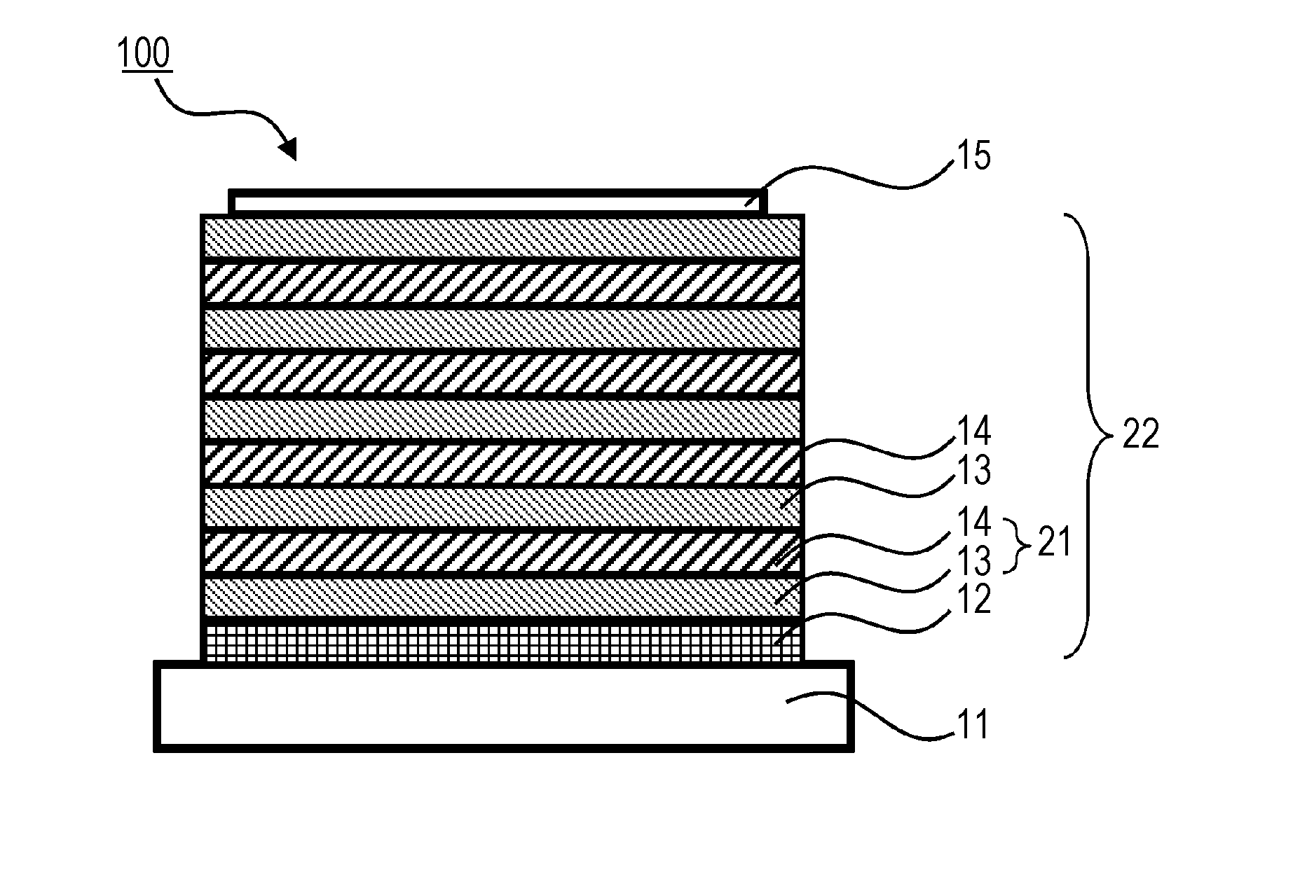
[0058]First, a BT solid solution polycrystalline film 12 of 50 nm was formed under conditions described below on a Pt plate of 10 mm×10 mm having a thickness of 1 mm and a surface flattened by polishing.

[0059]The BaTiO3 polycrystalline film 12 of 50 nm was formed by a sputtering method under the conditions including a target of BaTiO3, an atmosphere with an argon (Ar) / oxygen (O2) of 3 / 1, a pressure of 0.8 Pa, a high-frequency power of 200 W, and a substrate temperature of 200° C.

[0060]Then, annealing was performed at 800° C. in order to grow particles of the BT solid solution polycrystalline film 12 deposited on the Pt plate. The annealing temperature was over 600° C. and 1000° C. or less and preferably 800° C. or more and 1000° C. or less. In addition, annealing was performed in an oxidizing atmosphere in order to prevent a lack of oxygen in the BT solid solution polycrystalline film 12. Although, ...

examples 39 to 48

[0074]As in Examples 1 to 38, a BT solid solution polycrystalline film 12 of 50 nm was formed on a metal plate 11 (in the examples, a Ni plate) of 10 mm×10 mm having a thickness of 1 mm and a surface flattened by polishing, followed by annealing at 800° C.

[0075]The BT solid solution polycrystalline film 12 formed on the Ni plate as described above and a KN solid solution target having a composition shown in Table 1 were placed, and a KN solid solution film 13 having a thickness of 50 nm was formed by a sputtering method under the conditions including an atmosphere with an argon (Ar) / oxygen (O2) of 3 / 1, a pressure of 0.8 Pa, a high-frequency power 200 W, and a substrate temperature of 200° C., thereby forming a BaTiO3—KNbO3 solid solution two-layer film.

[0076]The BaTiO3—KNbO3 solid solution two-layer film formed as described above and a BT solid solution target having a composition shown in Table 1 were placed, and a KN solid solution film 14 having a thickness of 50 nm was formed by...

examples 49 to 58

[0081]Like in Examples 39 to 48, a BT solid solution polycrystalline film 12 of 50 nm was formed on a metal plate 11 (in the examples, a Ni plate) of 10 mm×10 mm having a thickness of 1 mm and a surface flattened by polishing, followed by annealing at 800° C.

[0082]The BT solid solution polycrystalline film 12 formed on the Ni plate as described above and a KN solid solution target having a composition shown in Table 1 were placed, and a KN solid solution film 13 having a thickness of 50 nm was formed by a PLD method under the conditions including a substrate temperature of 600° C., a laser power of 50 mJ, an O2 atmosphere as introduced gas, and a pressure of 33×10−3 Pa, thereby forming a BaTiO3—KNbO3 solid solution two-layer film.

[0083]The BaTiO3—KNbO3 solid solution two-layer film formed as described above and a BT solid solution target having a composition shown in Table 1 were placed, and a BT solid solution film 14 having a thickness of 50 nm was formed by a PLD method under the...


PUM

PropertyMeasurementUnit
thicknessaaaaaaaaaa
crystal grain diameteraaaaaaaaaa
thicknessaaaaaaaaaa

Abstract

The present invention provides a thin-film dielectric having a higher dielectric constant than usual ones and not requiring a special single crystal substrate, and also provides a large-capacity thin-film capacitor element using the thin-film dielectric.
A BaTiO3-based perovskite solid solution and a KNbO3-based perovskite solid solution are alternately formed to form a crystal structure gradient region where a lattice constant continuously changes at the interface, and thus crystal lattice strain occurs, thereby permitting the production of a thin-film dielectric having a high dielectric constant. Also, a large-capacity thin-film capacitor element can be produced by using the thin-film dielectric of the present invention.

Description

BACKGROUND OF THE INVENTION[0001]1. Field of the Invention[0002]The present invention relates to a thin-film dielectric and a thin-film capacitor element. In particular, the present invention relates to a thin-film dielectric capable of realizing a high dielectric constant and a thin-film capacitor element using the thin-film dielectric.[0003]2. Description of the Related Art[0004]Increases in density and integration of electronic circuits have been recently advanced with miniaturization and performance improvement of electronic apparatuses, and there have been demands for further miniaturization and thinning of capacitor elements serving as circuit elements which play important functions in various electronic circuits.[0005]On the other hand, clock rising time is shortened with increases in operating frequency of integrated circuits. Further, power supply voltages are further decreased for aiming at lower power consumption of apparatuses. Under these conditions, a rapid change in l...

Claims


Application Information

Patent Timeline
Patent Type & Authority Applications(United States)
IPC IPC(8): H01G4/30H01G4/10
CPCH01G4/10H01G4/306C04B35/49C04B35/495C04B2235/3201C04B2235/3203C04B2235/3208C04B2235/3213C04B2235/3215C04B2235/3251C04B2235/79C23C14/0036C23C14/08C23C14/088C23C14/28C23C18/1216C23C18/1225C23C18/125C23C18/1254H01G4/1227
Inventor FURUKAWA, MASAHITOKOSUDA, MASANORITAKEDA, SAORI
Owner TDK CORPARATION
Why Eureka
Try Eureka