Photocurable and thermocurable resin composition and dry film solder resist

a thermocurable resin and composition technology, applied in the field of thermocurable resin composition and dry film solder resist, can solve the problems of dimensional instability and warpage of components, affecting the life of the product, and dimensional instability or warpage has become a bigger problem, so as to improve thermal resistance reliability, improve thermal conductivity and electromagnetic wave absorption performance, and reduce the coefficient of thermal expansion

Active Publication Date: 2016-04-28
LG CHEM LTD
View PDF4 Cites 2 Cited by
  • Summary
  • Abstract
  • Description
  • Claims
  • Application Information

AI Technical Summary

Benefits of technology

[0021]The present invention has been made in an effort to provide a photocurable and thermocurable resin composition having advantages of having a lower coefficient of thermal expansion and improved thermal resistance reliability, and maintaining a magnetic property and a thermal conducting property, while simultaneously even imparting an electrical insulating property, thereby providing a dry film solder resist capable of implementing an excellent thermal conducting property and electromagnetic wave absorption performance without lowering voltage resistance strength.
[0022]Further, the present invention has been made in an effort to provide a dry film solder resist having advantages of having a lower coefficient of thermal expansion and improved thermal resistance reliability, and maintaining a magnetic property and a thermal conducting property, while simultaneously imparting an electrical insulating property, thereby implementing an excellent thermal conducting property and electromagnetic wave absorption performance without lowering voltage resistance strength.
[0061]Therefore, the DFSR may satisfy overall physical properties such as PCT resistance, TCT resistance, and HAST resistance between fine wires which are required for the substrate materials of a semiconductor device, and also reduce warpage, thereby reducing defects and increasing life of the product.
[0064]According to the present invention, there may be provided a dry film solder resist capable of having a lower coefficient of thermal expansion and improved thermal resistance reliability, and maintaining a magnetic property and a thermal conducting property, while simultaneously imparting an electrical insulating property, thereby implementing an excellent thermal conducting property and electromagnetic wave absorption performance without lowering voltage resistance strength, and a photocurable and thermocurable resin composition capable of providing the dry film solder resist.

Problems solved by technology

However, since each of the insulator, the semiconductor, and the conductor has a different coefficient of thermal expansion (CTE), dimensional instability and warpage of components are generated.
Such phenomenon generates a location mismatch between a chip and a substrate when connecting a chip die and a semiconductor substrate with a solder ball or a gold wire, and also generates cracks and breakage of the product due to shear strength, which may affect the life of the product.
As the thickness of the substrate has recently become gradually thinner, such dimensional instability or warpage has become a bigger problem.
Further, though an attempt has been made to lower the coefficient of thermal expansion of the solder resist by increasing the content of the filler to be used, when the content of the filler is increased above a certain level, a coating defect may occur due to aggregation of the filler, and an elongation rate may be decreased after coating before curing, thereby deteriorating workability.
However, the solder resist formed from the resin composition does not have a high glass transition temperature, and accordingly sufficient thermal resistance reliability, and thus does not properly meet PCT resistance, TCT heat-resistance, HAST resistance between fine wires, and the like which are required for package substrate materials of a semiconductor device.
In addition, as an integration degree of an electrical element is raised, an amount of generated electromagnetic waves is also increased, and these electromagnetic waves leak through a joining portion, a connecting portion, or the like of an electronic device, which lead to harmful effects such as causing a malfunction of other electrical elements or electronic components, or weakening an immune function of a human body.
Particularly, products in which a sheet having a thermal conducting property and a sheet having an electromagnetic wave shielding / absorbing performance are stacked have been widely used, but the products were thick due to the nature of the multilayered materials, had a problem in generation of an electrical short circuit and the like, and had difficulty in implementing the thermal conductivity and the electromagnetic absorbing property to the degree recently required by electronic devices.
Further, in order to improve the thermal conductivity and electromagnetic absorbing property, a method of increasing a charged amount of a filler added to the multilayered materials has been suggested, however, due to compatibility and the like, it is difficult to charge the filler above a certain amount, and when the charged amount of the filler is increased, hardness of the multilayered materials is increased, thereby reducing a thermal conducting property of the product.

Method used


Image

  • Photocurable and thermocurable resin composition and dry film solder resist
  • Photocurable and thermocurable resin composition and dry film solder resist
  • Photocurable and thermocurable resin composition and dry film solder resist

Examples


examples 1 to 3

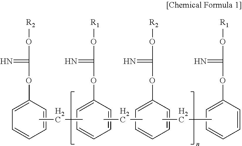
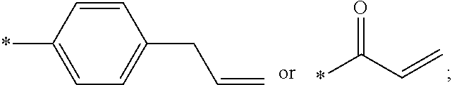
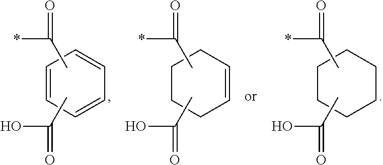
[0205]A bisphenol-based cyanate ester compound, BA-230 from Lonza, was used as an iminocarbonate-based compound of the acid-modified oligomer, and the cyanate group contained in the bisphenol-based cyanate ester compound, BA-230, was reacted with acrylic acid and 1,2,3,6-tetrahydrophthalic acid (4-cyclohexene-1,2-dicarboxylic acid) in a mole ratio of 1:1, thereby preparing an iminocarbonate compound which is the acid-modified oligomer.

[0206]45 g of this iminocarbonate-based compound was used, and 15 g of ZAR-2000 from Nippon Kayaku, Co., Ltd. as an additional acid-modified oligomer, 10 g of DPHA from SK Cytec Co., Ltd. as a photopolymerizable monomer, 2.5 g of TPO as a photoinitiator, 15 g of YDCN-500-80P from Nippon Kayaku, Co., Ltd. as a thermocurable binder, 0.25 g of 2-PI as a thermocurable binder catalyst, and an inorganic filler described in the following Table 1, 0.3 g of Phthalocyanine Blue as a pigment, 3.5 g of BYK-110 as a dispersant, and 20 g of DMF as a solvent were mix...

experimental examples

[0212]The physical properties of the dry films and the printed circuit boards manufactured in the above examples and comparative examples were measured in the following way.

experimental example 1

Developability (Sensitivity) Evaluation

[0213]A 12 μm copper foil laminated plate, from Mitsui Mining & Smelting Co., Ltd., was cut into a size of 5 cm×5 cm, and fine roughness was formed on the surface of the copper foil by chemical etching. After removing the release film from each dry film manufactured in the above examples and comparative examples, the film layer was vacuum-laminated on the copper foil laminated plate (substrate) where roughness is formed, with a vacuum laminator (MVLP-500, Meiki Co., Ltd.).

[0214]Then, a negative type of photomask having a hole shape with a diameter of 80 μm was closely adhered thereto, and exposed to UV having a wavelength range of 365 nm at an exposure amount of 350 mJ / cm2. Thereafter, the PET film was removed, and development with an alkaline solution of 1 wt % Na2CO3 at 31° C. was carried out for a certain period of time, thereby forming a pattern.

[0215]Then, the shape of the above-formed pattern was observed with SEM, thereby evaluating it a...


PUM

PropertyMeasurementUnit
diameteraaaaaaaaaa
weight ratioaaaaaaaaaa
Tgaaaaaaaaaa

Abstract

Provided are a photocurable and thermocurable resin composition including: an acid-modified oligomer including an iminocarbonate-based compound containing a carboxyl group and a photocurable unsaturated functional group; a photopolymerizable monomer having two or more photocurable unsaturated functional groups; a thermocurable binder having a thermally curable functional group; a functional filler including one or more selected from the group consisting of carbon allotrope particles having a ceramic compound bound to a surface thereof and heat radiating ceramic particles; and a photoinitiator, and a dry film solder resist manufactured therefrom.

Description

CROSS-REFERENCE TO RELATED APPLICATION[0001]This application claims the benefit of priority to Korean Patent Application No. 10-2014-0147657 filed in the Korean Intellectual Property Office on Oct. 28, 2014, the entire contents of which are incorporated herein by reference.TECHNICAL FIELD OF THE INVENTION[0002]The present invention relates to a photocurable and thermocurable resin composition, and a dry film solder resist.BACKGROUND OF THE INVENTION[0003]As various electronic devices are down-sized and reduced in weight, a photosensitive solder resist capable of forming a fine opening pattern is being used in a printed circuit board, a semiconductor package substrate, a flexible circuit board, and the like.[0004]A semiconductor package product is a composite material consisting of an insulator such as epoxy molding and a solder resist, a semiconductor such as a chip die, and a conductor such as a board circuit pattern, and in order to manufacture the product, various processes invol...

Claims


Application Information

Patent Timeline
Patent Type & Authority Applications(United States)
IPC IPC(8): G03F7/032
CPCG03F7/032
Inventor CHOI, BYUNG JUKYUNG, YOU JINJEONG, WOO JAECHOI, BO YUNLEE, KWANG JOOJEONG, MIN SU
Owner LG CHEM LTD
Why Eureka
Try Eureka