Conductive Adhesive with Spherical Graphene and Manufacturing Method thereof

Active Publication Date: 2016-09-29
SHENZHEN CHINA STAR OPTOELECTRONICS TECH CO LTD
View PDF3 Cites 6 Cited by
  • Summary
  • Abstract
  • Description
  • Claims
  • Application Information

AI Technical Summary

Benefits of technology

[0005]The invention is to provide a simple manufacturing method with abundant so

Problems solved by technology

However, there are some defects for this method: firstly, adhesion and homogeneity of the nickel plating maybe affected due to sensitization of polymer materials to absorb some tin ions; secondly, based on Autoctalytic Deposition for this case, Au(CN)2−+Ni→Au+Ni2++2CN—, the nickel ions exists automatically, and to control the plating layer for the crystal layer, cobalt ions is added in the action, furthermore, the defect is that polymer material

Method used


Image

  • Conductive Adhesive with Spherical Graphene and Manufacturing Method thereof
  • Conductive Adhesive with Spherical Graphene and Manufacturing Method thereof

Examples


Embodiment Construction

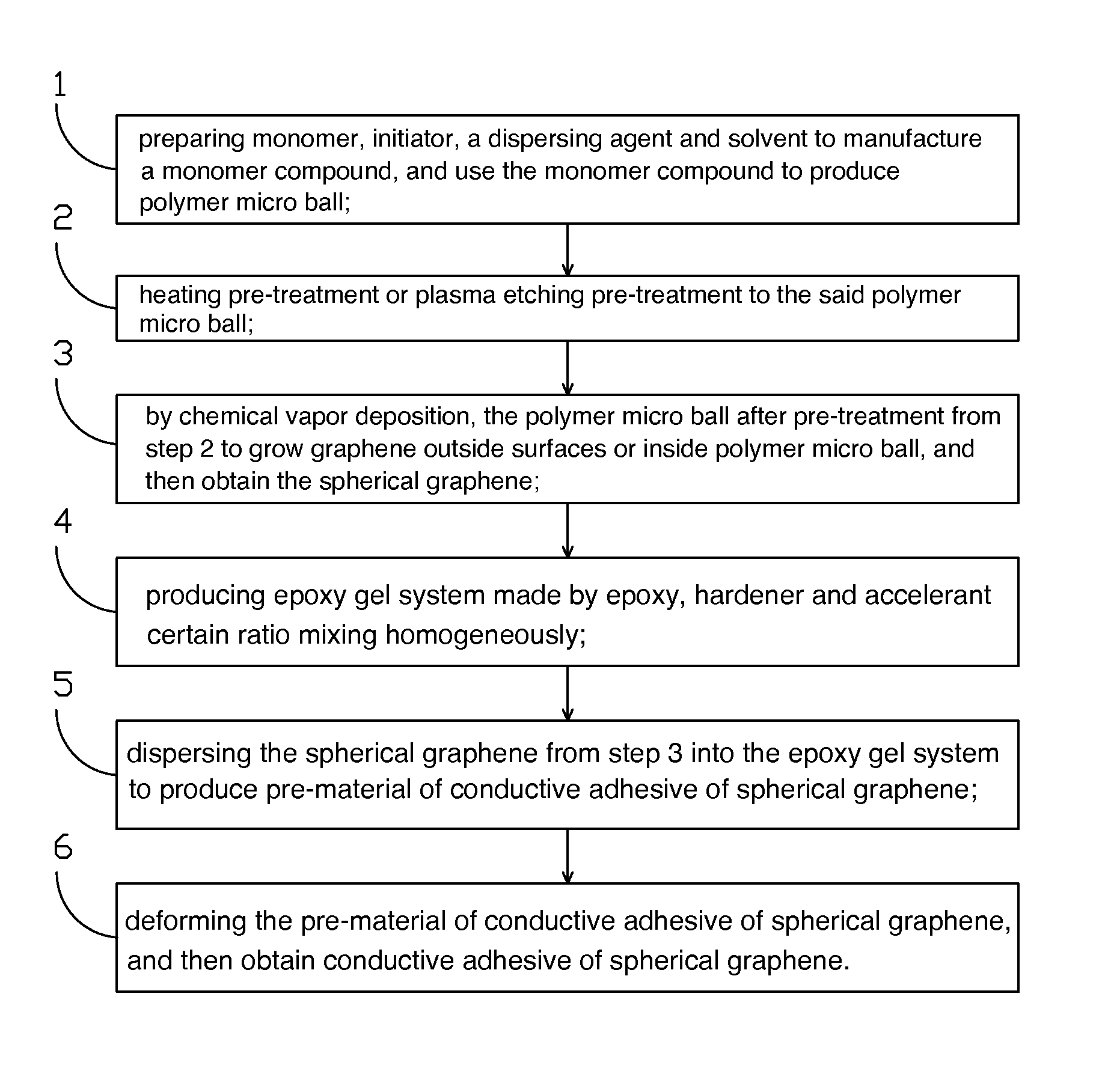
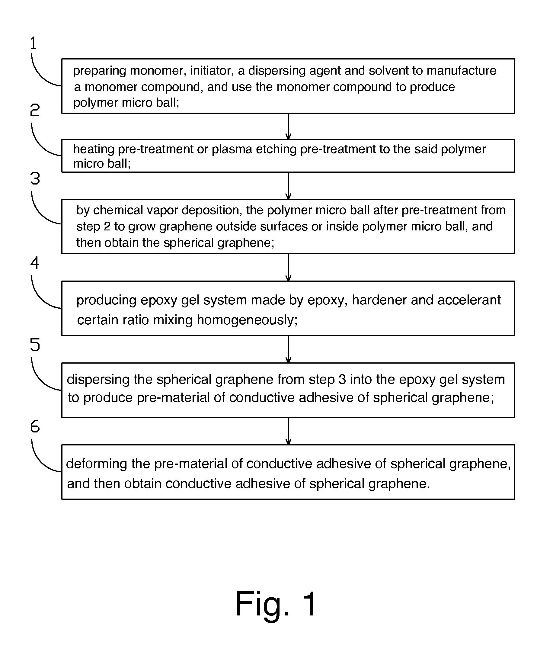
[0045]Reference will now be made in detail to example embodiments, examples of which are illustrated in the accompanying drawings, wherein like reference numerals refer to like elements throughout. In this regard, the present example embodiments may have different forms and should not be construed as being limited to the descriptions set forth herein. Specific structural and functional details disclosed herein are merely representative for purposes of describing example embodiments, and thus may be embodied in many alternate forms and should not be construed as limited to only example embodiments set forth herein. Therefore, it should be understood that there is no intent to limit example embodiments to the particular forms disclosed, but on the contrary, example embodiments are to cover all modifications, equivalents, and alternatives falling within the scope of the disclosure.

[0046]As shown in FIG. 1, the invention provides a manufacturing method for producing conductive adhesive ...


PUM

PropertyMeasurementUnit
Fractionaaaaaaaaaa
Fractionaaaaaaaaaa
Fractionaaaaaaaaaa

Abstract

The invention provide a manufacturing method for producing conductive adhesive with spherical graphene, and the steps comprise as following: step 1: preparing monomer, initiator, a dispersing agent and solvent to manufacture a monomer compound, and use the monomer compound to produce polymer micro ball; step 2: heating pre-treatment or plasma etching pre-treatment to the said polymer micro ball; step3: by chemical vapor deposition, the polymer micro ball after pre-treatment from step 2 to grow graphene outside surfaces or inside polymer micro ball, and then obtain the spherical graphene; step 4: producing epoxy gel system made by epoxy, hardener and accelerant with a certain ratio mixing homogeneously; step 5: dispersing the spherical graphene from step 3 into the epoxy gel system to produce pre-material of conductive adhesive of spherical graphene; Step 6: deforming the pre-material of conductive adhesive of spherical graphene, and then obtain conductive adhesive of spherical graphene.

Description

FIELD OF THE INVENTION[0001]The invention relates to Liquid Crystal Display (LCD) field, especially to a conductive adhesive with spherical graphene and a manufacturing method thereof.BACKGROUND OF THE INVENTION[0002]Usually thin film transistor liquid crystal display (TFT-LCD) arrange all tapping electrode on one side, electronically co-connect array side and CF side to the same glass substrate by conductive point, and drive chip attached on said substrate. The conductive point is usually composed of thermalsetting epoxy resin, glass fibers and 1 wt %˜2 wt % Au ball. Au ball is based on a spherical elastic material (ex: Acrylic acid) by plating a layer of Nickel firstly, and then plating Gold afterword. Being an elastic conductivity micro ball, the radius is usually from 5 to 8 μm, and conductivity reaches to 2.4×10⁵Scm−1. Procedures of traditionally manufacturing Au balls need to induce active targets at chemical reactions on surface of basal body via cleaning, light etching, sens...

Claims


Application Information

Patent Timeline
IPC IPC(8): C09J9/02C23C16/26C23C16/48H01B1/24B01J2/06B01J2/00C23C16/44C09J163/00C23C16/02
CPCC09J9/02C09J163/00C23C16/26C23C16/481H01B1/24C23C16/0245B01J2/06B01J2/003C23C16/4417C23C16/0209C01P2004/32C01B32/186C08K9/12C08K2201/001C08K3/042C08J7/00C09J11/04C09J2203/326C09J2400/10C09J2463/00C09J11/00C01B32/194
Inventor LEE, YUNGJUIZHANG, XIALI, JICHEN, YAHUI
Owner SHENZHEN CHINA STAR OPTOELECTRONICS TECH CO LTD
Why Eureka
Try Eureka