Super-high aspect ratio diffractive optics fabricated by batch-processing

a batch processing and diffractive optic technology, applied in the field of diffractive optics, can solve the problems of insufficient x-ray or particle beam focusing efficiency, the modest aspect ratio of the features that all these types of lithography and methods can produce, and the inability to fabricate self-standing geometric objects of this aspect ratio without collapse or distortion, etc., to achieve fine tuning of optical properties, improve efficiency, and improve mechanical, thermal and electrical properties of devices

Active Publication Date: 2019-05-23
ALCORIX CO
View PDF0 Cites 13 Cited by
  • Summary
  • Abstract
  • Description
  • Claims
  • Application Information

AI Technical Summary

Benefits of technology

[0056]Optional post-processing is possible and can lead to enhancement of the mechanical, thermal, and electrical properties of the devices, or can be used to fine tune their optical properties. The method can be readily generalized for nanolaminates comprising multilayer stacks of ALD films, M1, M2 . . . MN, to approach a smooth variation of absorbance and of phase shifting across Fresnel zones, for an increase in efficiency and the elimination of unwanted focusing and diffraction orders. Optional post processing for integrating other X-ray optical components or integrating the X-ray optics into more complex micro-electro-mechanical systems is possible.

Problems solved by technology

Self-standing geometric objects of this aspect ratio are essentially impossible to fabricate without collapse or distortion at this time.
The limitations of all these types of lithography and methods are the modest aspect ratios of the features that they are capable of producing.
These aspect ratios are insufficient for efficient focusing of x-rays, or particle beams of a corresponding energy.
Metal-enhanced chemical etching (MACE) of silicon (Si) was reported by C. Chang and A. Sakdinawat (Nature Communications 5, 4243, (2014)) to obtain zone plates with aspect ratios as high as 40:1, but inherent difficulties are encountered with large scale uniformity and reproducibility, while the material used is restricted to Si, which has a too high absorption for a scaffold material and too low refraction index for a phase shifter material.
One drawback of this method is the accentuation or amplification of radius irregularities of the central wire (i.e. the roughness or accidental other variations including particulate defects and thickness variations during the deposition) as successive layers are deposited beginning from the bare wire and proceeding to the outermost layer.
A second drawback is the accumulation of the absolute error values of the deposition thicknesses of each of the inward layers as an error of placement of the next outward layer.
Thus, the outermost (i.e. thinnest) layers accumulate the largest radius errors due to the amplification and accumulation of the depositional processes errors through successive layers.
This error amplification process can produce defects in the final (thinnest) zone shape and placement exceeding a half-width of the layer / zone itself, rendering that portion of the diffractive line useless for focusing or adequate manipulation of phase shift of the prescribed photon or particle beam.
However, in order to effectively reduce the error amplification process, the slit widths have to be reduced to fractions of the wire diameter, which reduces the deposition rate to impractically low values.
Another drawback of the sputter-and-slice method is that only one wire can be processed at a time, while the slicing / polishing procedures are serial and time-consuming.
The method suffers from the same drawbacks as the wire-based version and can be used only for linear (one-dimensional) optics; however, it has shown relatively higher rates of success because it is easier to obtain highly planar and smoothly-polished planar surfaces rather than perfectly circular, low roughness wires or tubes.
However, this method still preserves error accumulation in layer thicknesses, but these errors are more easily kept in control, due to the more precise nature of the ALD process.
An additional drawback of the ALD-and-slice method is the relative slow rate of deposition in ALD processes, which require months-long deposition times for Fresnel Zone Plates with a reasonable number of zones.
In practice, for deposition by sputtering, this fabrication process would be limited by the variation of thickness of sputtered layers with the depth in the hole, inherent to the sputtering process.
As mentioned above, while sequential ALD is capable of deposition of conformal layers of uniform and controlled thickness, in practice, the method of Yun et al. would be limited by the surface roughness of the cylindrical holes, which depends on the etch process used for etching the holes.
Thus, the thickness of the thinnest functional zone of the diffractive optic is limited by the average roughness of the side walls, which is usually tens or hundreds of nm for most etching processes.
This accuracy is difficult to characterize in holes of the required depth and aspect ratio, except by destructive procedures.

Method used


Image

  • Super-high aspect ratio diffractive optics fabricated by batch-processing
  • Super-high aspect ratio diffractive optics fabricated by batch-processing
  • Super-high aspect ratio diffractive optics fabricated by batch-processing

Examples


first embodiment

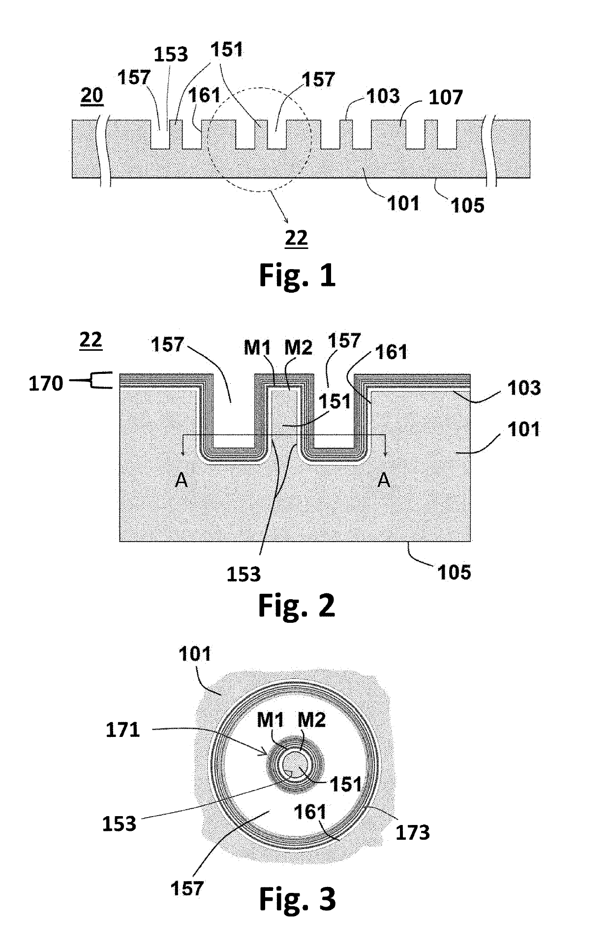
[0081]FIGS. 1 to 10 illustrate schematically steps in a batch processing method of fabricating a device structure comprising a high aspect ratio diffractive optic comprising a Fresnel Zone Plate (FZP).

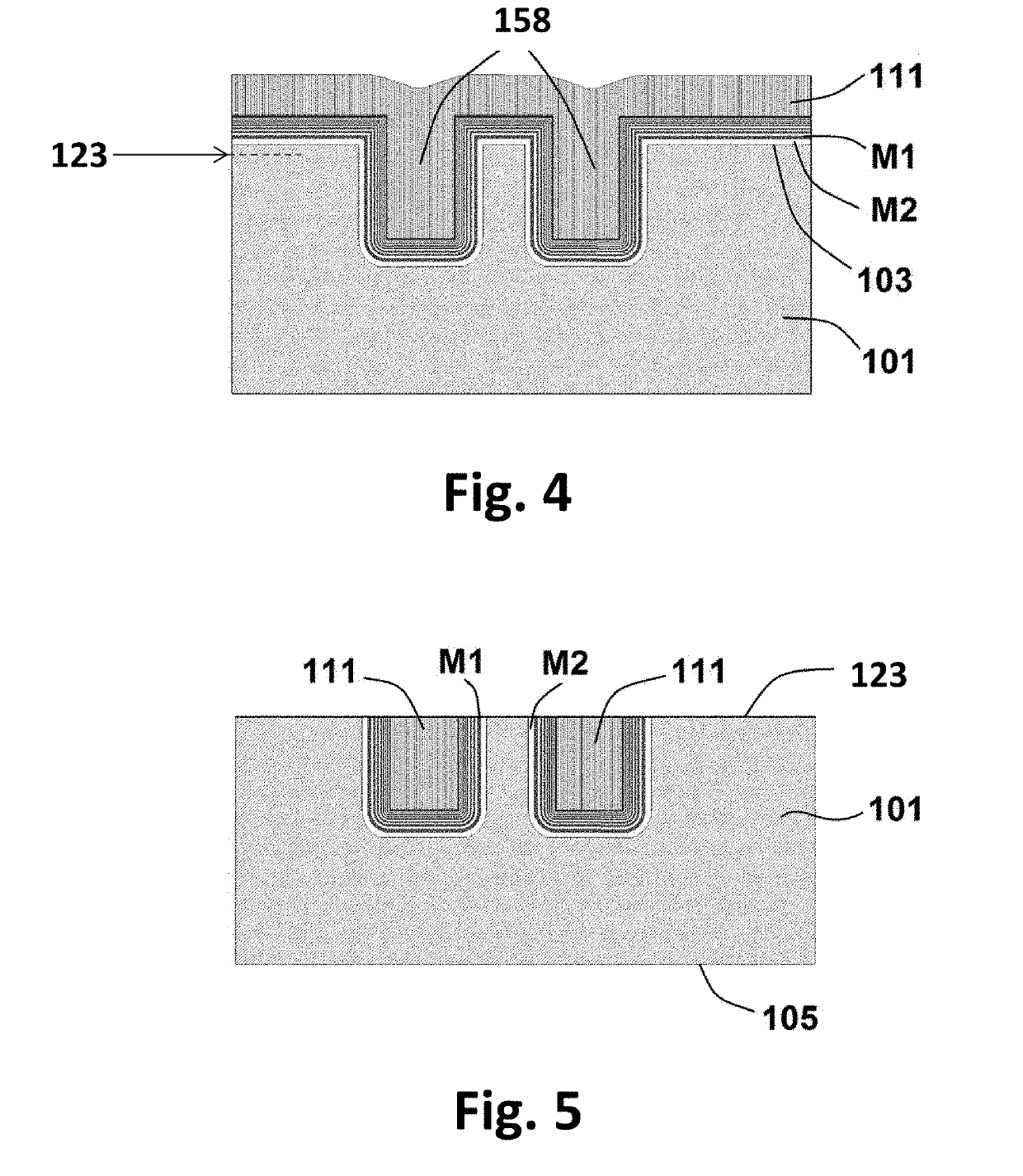
[0082]FIG. 1 shows a schematic cross-sectional view part of a precursor structure 20 comprising an array of cylindrical columns 151 defined in a planar substrate 101. Each column 151 is formed within a surrounding, concentric, cylindrical recess 157, with the sidewall 161 of the recess spaced from the sidewall 153 of the column. The planar substrate comprises, for example a silicon wafer having a smooth polished planar front surface 103 and back surface 105. FIG. 2 shows an enlarged view of part 22 of FIG. 1, comprising one of the array of cylindrical columns 151 within its recess 157, after deposition of a nanolaminate 170 comprising a sequence of conformal layers, comprising a first material M1 and a second material M2. As illustrated schematically, the nanolaminate 170 comprises a ...

fourth embodiment

[0135]Thus, FIG. 16A shows a schematic cross-sectional view of a multiple-phase diffractive optics device of a fourth embodiment, comprising a FZP for hard X-rays, using multiple layers (N) stacks of materials M1, M2, . . . MN. FIG. 16B illustrates the resulting N-steps phase shift approximation corresponding to an ideal continuous-varying phase shift in a kinoform as shown in FIG. 17C. Thus, it will be appreciated that the method can be readily generalized for multilayer stacks of ALD films, M1, M2, . . . MN, to approach a smooth variation of absorbance of phase shifting across Fresnel zones, for an increase in efficiency and elimination of unwanted focusing / diffraction orders.

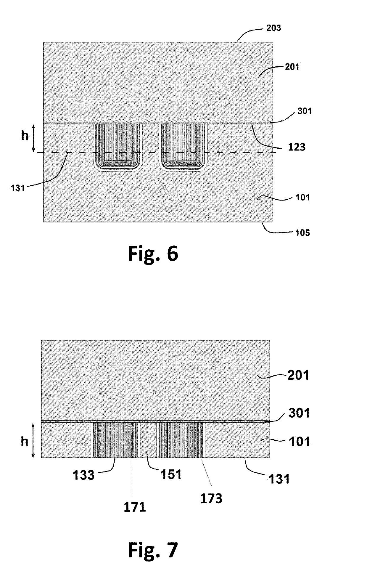
[0136]In the device structures of the embodiments described in detail above with reference to FIGS. 1 to 17, the diffractive optics comprise diffractive line patterns in the form of concentric circular zones, formed around a cylindrical column or pillar. By providing a precursor structure or form comprising a...

second embodiment

[0147]For example, a certain tilt angle or other structuring of the side walls of structures used to deposit the sequential ALD layers is possible, allowable, and potentially advantageous to the functioning of the diffractive optical devices so fabricated, as long as the slant angle and other geometrical parameters of the resultant device are well controlled. For example, a tilt angle or slope of the sidewalls of the columns for the device structure of second embodiment, could lead to an enhancement of the focusing efficiency in a certain focus spot corresponding to a focus order towards which the tilted zone is pointing / blazing. Variations of the tilt angle close to this blazing direction can provide “guiding” of the hard X-rays or particle beams by channeling them in those directions, as long as the reflections on the adjacent zone walls are close to the total reflection condition. Recently, an analogous effect of guiding of X-rays through curved (similar to tilted) micro-channels...


PUM

PropertyMeasurementUnit
thicknessaaaaaaaaaa
thicknessaaaaaaaaaa
energyaaaaaaaaaa

Abstract

A batch processing method for fabrication of diffractive optics is disclosed, having applicability to high resolution ultra-high aspect ratio Fresnel Zone Plates for focusing of X-rays or gamma-rays having energies up to hundreds of keV. An array of precursor forms comprising columns is etched into a planar substrate. After sidewall smoothing, a nanolaminate, comprising a sequence of alternating layers of different complex refractive index, is deposited on the sidewall of each column by atomic layer deposition (ALD), to define a specified diffractive line pattern around each column, to form a binary or higher order diffractive optic. After front surface planarization and thinning of the substrate to expose first and second surfaces of the diffractive line pattern of each diffractive optic, the height h in the propagation direction provides a designed absorption difference and/or phase shift difference between adjacent diffractive lines. Optionally, post-processing enhances mechanical, thermal, electrical and optical properties.

Description

CROSS REFERENCE TO RELATED APPLICATION[0001]This application is a continuation-in-part of U.S. patent application Ser. No. 15 / 363,950, filed Nov. 29, 2016, entitled “Batch-Processing Method for Super-High Aspect Ratio Diffractive Optics”, which claims priority from U.S. Provisional patent application No. 62 / 302,352, filed Mar. 2, 2016, entitled “Batch-Processing Method for Super-High Aspect Ratio Diffractive Optics”; both applications are incorporated herein by reference in their entirety.FIELD OF THE INVENTION[0002]This invention relates to diffractive optics and a method of manufacturing high aspect ratio diffractive optic devices applicable to the focusing or shaping of wave fronts of very high energy electromagnetic radiation or particle beams using curved or variable-spaced diffractive lines of absorber or phase shifter materials, with sub-20 nm features and aspect ratios up to tens of thousands to one.BACKGROUND[0003]Many diffractive optics devices, such as those used for focu...

Claims


Application Information

Patent Timeline
Patent Type & Authority Applications(United States)
IPC IPC(8): G02B5/18H01L21/321H01L21/768G02B3/08G21K1/06C23C16/455
CPCG02B5/1876H01L21/32115H01L21/7684G02B3/08G21K1/062G21K1/067C23C16/45555G21K2201/067
Inventor MOLDOVAN, NICOLAIE A.
Owner ALCORIX CO
Why Eureka
Try Eureka