Three-dimensional scanning lidar based on one-dimensional optical phased arrays

a phased array, three-dimensional scanning technology, applied in the field of light detection and ranging (lidar), can solve the problems of limiting the improvement of detection speed, affecting the efficiency of automatic driving system, so as to achieve the effect of reducing the burden on the rear-end data processing circuit and the entire automatic driving system, stable operation, and reducing the complexity of cost and control circuits

Pending Publication Date: 2021-01-21
SHANGHAI JIAO TONG UNIV
View PDF0 Cites 12 Cited by
  • Summary
  • Abstract
  • Description
  • Claims
  • Application Information

AI Technical Summary

Benefits of technology

[0039]1. By adopting transceiving complexity decomposition, the present invention decompose the quadratic relation O(n2) between the element complexity and scanning resolution required by three-dimensional scanning into two groups of linear relations O(2n), i.e., of the transmitting end and the receiving end mutually orthogonal to each other; single-wavelength three-dimensional scanning can therefore be realized or multi-beam application can be realized with additional wavelength resources. The transceiving array with linear complexity and the linear photodetector array have remarkable advantages in cost and control circuit complexity.
[0040]2. The present invention does not contain any moving parts, the limitation of the angular refreshing rate is completely determined by the physical limit of light propagation between the LiDAR and the target, and by hitchhiking along with the development of the integrated optical communication technology, the required thermo-optic or electro-optic phase shifters or other phase shifters can be further improved in the aspects of power consumption, operation speed etc. Meanwhile, as an strict solid-state device, mechanical abrasion or deformation does not exist in the system, and stable operation can be maintained in an environment with rapid acceleration or deceleration.
[0041]3. The present invention realize a pure solid-state three-dimensional scanning LiDAR, wherein the beam forming directions of two adjacent operating instants are independent from each other and are digitally controlled by the mast computer, so that detection resources can be flexibly allocated in the field of view, subsequently realizing intelligent detection with the capability to focus on high-value target. The burden on the rear-end data processing circuit and on the entire automatic driving system can be effectively reduced.
[0042]4. According to the present invention, the cost of optical phased array chips can be significantly reduced through large-scale batch production by means of semiconductor optoelectronic co-integration process; in addition, the present invention has the characteristic of modularization, supports different types of light sources and peripheral control circuits. The invention can not only realize an integrated chip system design, but also can form a distributed system by using a plurality of terminal sensors pairs matched with a single high-performance host where light source and control circuits are concentrated.

Problems solved by technology

As the mechanical system has moving parts, issues such as mechanical wear, structural reliability, precision in motion control, and the influence of inertia in acceleration environment, make it difficult for the mechanical scanning scheme to achieve high-speed and large-angle beam rotation at the same time.
In addition, the mechanical scanning solutions suffer significantly in terms of volume and power consumption.
However, the hybrid solid-state systems still contain moving parts, moreover, they face significant resonance and deformation problems in high-speed operation, which limit the improvement in detecting speed.
In addition, as the mechanical scanning is a continuous process and the detection directions at two adjacent instants cannot be abruptly changed, the detection resources cannot be flexibly allocated.
On the other hand, non-scanning LiDAR, which is similar to the camera in principle, can not allocate detection resources flexibly either.
As the complexity of the array scaled quadratically in relation to the detection fineness, it is difficult for the solution to realize high-resolution and high-real-time environment sensing at the same time.
Finally, as the “laser flash” needs to illuminate the entire field of view, in a medium to long working distance required for automatic driving applications, such solution creates another pair of trade-off between sensor cost and detection range.
On one hand, this publication demonstrated the feasibility to realize large scale OPAs with the state-of-art fabrication process as well as the beam-forming flexibility of an OPA; on the other hand, the issues related to the control complexity of two-dimensional phased arrays is exposed as well.
Although the patent did not use a wavelength tunable laser, as the number of lines increases, the switch size, the number of subarrays, and the complexity of the control circuit amount to large scale and high cost, and eventually will again reaching a complexity of O(n2).
Therefore, the architecture will be limited with a tradeoff between the number of available resolvable points, the overall complexity, and the on-chip insertion loss.
However, since the angular resolution of the phased array is inversely proportional to the total size of the phased array, the total number of antennas inside a high-density integrated OPA can reach thousands to tens of thousands in order to compete with the collimation system in traditional scanning LiDAR with respect to far field resolution, and subsequently the complexity of the control circuit and the burden of the master computer are greatly increased.
Because the refractive index difference between the core layer and the cladding layer of the III / V platform waveguide is much smaller than that of silicon platform, the mode distribution in the III / V dielectric waveguide is wider, the device size and bending radius are both larger, the evanescent coupling between channels is more serious, and the unit area cost of a III / V chip is significant.
Due to the issues above, the theoretical performance of this platform is not appealing to chip design, and there is no significant advantage to integrate the optical phased arrays on III / V platform.
However, the issues with this standard architecture are significant.
Meanwhile, as the angle tuning efficiency of the grating antenna is generally limited, the laser needs to tunable over a wide-range of wavelength.
Note that these performance requirements should be met simultaneously, while it must be feasible on the C-band integrated optical platform originally optimized for optical communication applications, therefore, the cost of such a laser is obviously significant due to various rigorous requirements.
In addition, since the number of resolvable points for the corresponding direction of wavelength tuning is directly proportional to the number of periods of the grating antenna, which may need to reach several centimeters in order to achieve lower beam divergence, for a grating antenna of that length, process errors will result in the accumulation of random phase errors and significant losses.
Moreover, when these long antennas are juxtaposed to form a phased array, the finite mode field confinement of dielectric waveguides will result in phase crosstalk between adjacent channels, and subsequently resulting in a tradeoff between the effective scanning range in the direction scanned by the phased array and the effective beam divergence in the direction scanned by the grating antenna.
Finally, the passive grating antenna array also occupies a large chip area, and the overall cost of the chip system is relatively high.

Method used


Image

  • Three-dimensional scanning lidar based on one-dimensional optical phased arrays
  • Three-dimensional scanning lidar based on one-dimensional optical phased arrays
  • Three-dimensional scanning lidar based on one-dimensional optical phased arrays

Examples


Embodiment Construction

[0058]The present invention is described in further detail with reference to the drawings and examples. The following specific examples are for illustrative purposes only and are not intended to limit the present invention. At the same time, the technical features involved in different implementations in the embodiments may be combined with each other as long as there is no theoretic conflict in implementation.

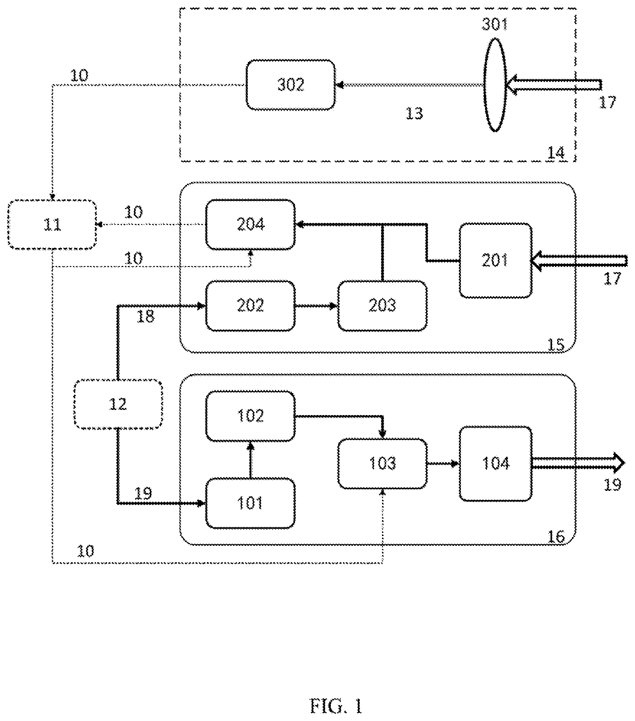
[0059]As shown in FIG. 1, the three-dimensional scanning LiDAR based on one-dimensional optical phased arrays comprises a narrow line width laser light source and a high-speed integrated circuit controller, and is characterized by further comprising a transmitting end Tx 16, a coherent receiving end Rc 15, and an incoherent receiving end Ri 14, the transmitting end Tx 16 comprising a detection light input waveguide 101, a first beam splitter module 102, a phase shifter array module 103, and a coupling suppressed one-dimensional transmitting array of sub-wavelength pitch 104 in...


PUM


Abstract

A three-dimensional scanning LiDAR based on one-dimensional optical phased arrays comprises a transmitting end, a coherent receiving end and an incoherent receiving end, wherein the transmitting end, the coherent receiving end and the incoherent receiving end are all one-dimensional arrays. A phase control complexity of the three-dimensional scanning phased array is reduced, and a tunable laser with high cost and a grating array antenna with large crosstalk are avoided. The LiDAR provides pure solid-state three-dimensional scanning in speed and integration level and is highly practical.

Description

CROSS-REFERENCE TO RELATED APPLICATIONS[0001]The subject application is a continuation of PCT / CN2019 / 087748 filed on May 21, 2019, which claims priority on Chinese Application No. CN201910367089.8 filed on May 5, 2019 in China. The contents and subject matter of the PCT international application and the Chinese priority application are incorporated herein by reference.TECHNICAL FIELD[0002]The present invention belongs to the field of light detection and ranging (LiDAR), and particularly relates to a three-dimensional scanning LiDAR based on a one-dimensional optical phased arrays (OPAs).BACKGROUND ART[0003]As the automatic driving technology evolves, its applications in Advanced Driving Assistant System (ADAS) and Robotic Cars are coming to the critical stage of marketization. Accurate real-time sensing of the environment around a vehicle is not only an application requirement but also a key factor for traffic safety and market confidence. Under the background of sensor fusion, the ...

Claims


Application Information

Patent Timeline
Patent Type & Authority Applications(United States)
IPC IPC(8): G01S7/481G01S17/42
CPCG01S7/4815G01S17/42G01S7/4817Y02A90/10
Inventor LU, LIANGJUNXU, WEIHANZHOU, LINJIECHEN, JIANPINGLIU, JIAO
Owner SHANGHAI JIAO TONG UNIV
Why Eureka
Try Eureka