

Optoelectronic synaptic memristor
a synaptic memristor and optoelectronic technology, applied in the field of optoelectronic synaptic memristor, can solve the problems of not being able to meet the development needs, not being able to realize intelligent data and information processing, and not being able to real-time and self-adaptive evolution to meet the changing application scenarios and demands, etc., to achieve the effect of accelerating the application of optoelectronic synaptic devices and overcoming
- Summary
- Abstract
- Description
- Claims
- Application Information
AI Technical Summary
Benefits of technology
Problems solved by technology
Method used
Image

Examples
embodiment 1
Preferred Embodiment 1
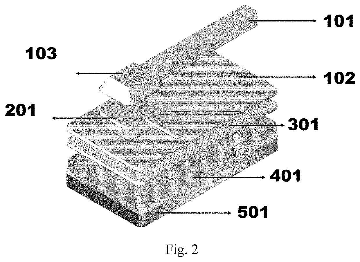
[0038]According to the preferred embodiment 1 of the present invention, as shown in FIG. 2, an optoelectronic synaptic memristor is provided, comprising a silicon nitride waveguide layer (Si3N4) 101 with a wedge-shaped output terminal 103, an oxide isolation layer (SiO2) 102, a transparent top electrode layer (ITO) 201, a two-dimensional material layer made of molybdenum disulfide and molybdenum oxide (MoS2 / Mo2-xOx) 301, a porous silicon oxide structure layer modified with graphene quantum dots (GQDs@PSiOx) 401, and a bottom electrode layer (Si) 501, which are arranged in sequence from top to bottom.
[0039]The waveguide layer (without the wedge-shaped output terminal) has a width of 5 μm and a height of 10 μm; an inclination angle of each side of the wedge-shaped output end is 45°, and a contact surface of the wedge-shaped output end with the transparent top electrode layer is 10*10 μm2; the transparent top electrode layer has a thickness of 200 nm; the two-dime...
embodiment 2
Preferred Embodiment 2
[0051]According to the preferred embodiment 2 of the present invention, as shown in FIG. 2, an optoelectronic synaptic memristor is provided, comprising a silicon waveguide layer (Si) 101 with a wedge-shaped output terminal 103, an oxide isolation layer (SiO2) 102, a transparent top electrode layer (FTO) 201, a two-dimensional material layer made of black phosphorus (BP) 301, a silicon porous structure layer modified with β-NaYF4:Yb3+, Tm3+ / NaYF4 quantum dots (β-NaYF4:Yb3+, Tm3+ / NaYF4@PSi) 401, and a bottom electrode layer (Si) 501, which are arranged in sequence from top to bottom.
[0052]The waveguide has a width of 2.5 μm and a height of 5 μm; an inclination angle of each side of the wedge-shaped output end is 45°, and a contact surface of the wedge-shaped output terminal with the transparent top electrode layer is 5*5 μm2; the transparent top electrode layer has a thickness of 100 nm; the two-dimensional material layer, namely a BP layer, has a thickness of 3...
embodiment 3
Preferred Embodiment 3
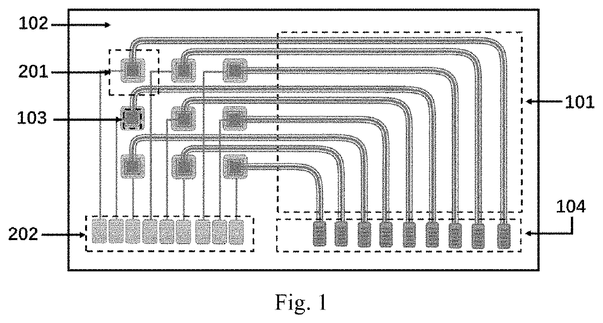
[0059]Referring to FIG. 1, the preferred embodiment 3 provides an optoelectronic synaptic device array, comprising: N*M optoelectronic synaptic memristors (N≥1 and M≥1). Each of the optoelectronic synaptic memristors comprises: a silicon nitride waveguide layer (Si3N4) 101 with a wedge-shaped output terminal (Si3N4) 103, an oxide isolation layer (SiO2) 102, a grating coupler (Si3N4) 104, a transparent top electrode layer (ITO) 201, an external electrode (Au) 202 connected to the top electrode, a two-dimensional material layer (MoS2 / Mo2-xOx) 301 located below an oxide isolation layer, which is made of molybdenum disulfide and molybdenum oxide, a porous silicon oxide structure layer modified with graphene quantum dots (GQDs@PSiOx) 401, and a bottom electrode layer (Si) 501.
[0060]According to the preferred embodiment 3, the optoelectronic synaptic device array is obtained by integrating the waveguides and the optoelectronic memristors structure. All the optoelectr...
PUM
| Property | Measurement | Unit |
|---|---|---|
| inclination angle | aaaaa | aaaaa |
| height | aaaaa | aaaaa |
| width | aaaaa | aaaaa |
Abstract
Description
Claims
Application Information