

Method of manufacturing semiconductor devices using a crystallization promoting material
a technology of crystallization promotion and manufacturing method, which is applied in the direction of semiconductor devices, electrical equipment, instruments, etc., can solve the problems of reproducibility and stability problems, adversely affecting the electric characteristic and reliability of tft, and the inability to use an amorphous silicon film as an active layer
- Summary
- Abstract
- Description
- Claims
- Application Information
AI Technical Summary
Benefits of technology
Problems solved by technology
Method used
Image

Examples
second embodiment
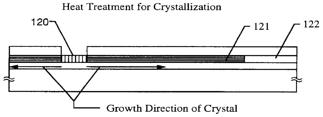
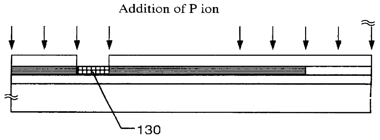
This embodiment is completely identical with the first embodiment in processes of from the P ion adding process to the heating process (FIG. 2A). Also, FIG. 3A is identical with FIG. 2A.
In the first embodiment, because HCl added gas is used as gas containing halogen elements in the inactive gas atmosphere, the silicon film existing under the insulating film mask is also removed as shown in FIG. 2B.
Therefore, in this embodiment, the silicon film in the nickel added region is etched through wet etching using buffer hydrofluoric acid (or hydrofluoric acid etchant) or dry etching as another process. Thereafter, using HCl added gas as gas containing halogen elements in an oxidizing gas atmosphere, a gettering process is made from the etched section of the silicon film.
In this example, Cl is selected as halogen elements, and HCl is used as its introducing method. As a gas other than HCl, one or plural kinds of gases selected from HF, HBr, Cl.sub.2, F.sub.2 and Br.sub.2 can be used. Also, ...
third embodiment
This embodiment is completely identical with the first embodiment in processes of from the P ion adding process to the heating process (FIG. 2A) except that a quartz substrate is used as a substrate 100. Also, FIG. 4A corresponds to FIG. 2A.
In the second embodiment, because HCl added gas is used as gas containing halogen elements in the oxidizing gas atmosphere, an oxide is liable to abnormally grow.
Accordingly, in this embodiment, as another process, after the phosphorus added region is removed, the insulating film mask is removed, and patterning is made to obtain an island-like silicon film. Then, after a silicon oxide film 180 is laminated on the entire surface of the film to cover the island-like silicon film, a heat treatment is conducted under an oxidizing atmosphere in which halogen elements are added to thereby smooth the surface of the insulating film. Hereinafter, this process will be described in more detail.
First, the silicon film in the phosphorus added region 140 is et...
fourth embodiment
In this embodiment, an example of a process of producing a CMOS circuit in which an N-channel TFT and a P-channel TFT are complementally combined together will be described.
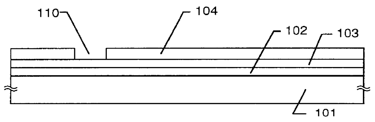
In FIG. 6A, reference numeral 301 denotes a glass substrate; 302 is an under film; 303 is an active layer of an N-channel TFT; and 304 is an active layer of a P-channel TFT. The active layers 303 and 304 are produced according to the manufacturing process described in the first to third embodiments.
Then, a silicon oxide film is formed in thickness of 150 nm through the plasma CVD method or the low pressure CVD method to form a gate insulating film 305 (FIG. 6A).
Thereafter, a metal film mainly containing aluminum is formed (not shown), and an original of a gate electrode which will be formed later is formed by patterning. Then, the technique disclosed in Japanese Patent Unexamined Publication No. Hei 7-135318 by the present inventors is employed. The disclosure of this patent is incorprated herein by reference. Th...
PUM
| Property | Measurement | Unit |
|---|---|---|
| temperature | aaaaa | aaaaa |
| crystallization temperature | aaaaa | aaaaa |
| thickness | aaaaa | aaaaa |
Abstract
Description
Claims
Application Information