
Layered metal foil semiconductor power device

a technology of power devices and metal foils, applied in the direction of basic electric elements, electrical equipment, radiation applications, etc., can solve the problems of large and massive apparatuses, low power density, and no other technology has seen substantial commercial application, and achieve the effect of greater power and greater energy

Inactive Publication Date: 2000-09-12
BROWN PAUL M
View PDF12 Cites 65 Cited by
  • Summary
  • Abstract
  • Description
  • Claims
  • Application Information

AI Technical Summary

Benefits of technology

Other objects of the present invention are to provide a new power source which will operate at low temperatures, have very long working life, and be unaffected by vibrations or acceleration.
Other objects of this invention is to provide a new power source which will not be damaged by an accidental short circuit, and which is light and small in size, relative to the energy it produces.
Another object of this invention is to provide a power source which is very rugged and extremely reliable; unaffected by environments such as vacuums, high pressures, corrosive atmospheres, and undamaged by temporary exposures to high temperatures.
The preferable tritium-doped semiconductor region essentially "locks" the electron bands in place, whereby the converter surfaces can be treated in any manner desired without degrading device performance. In such an arrangement, ohmic contacts can easily be made to the converter surfaces. In fact, any adjacent oxide layers formed thereon will not alter the electron band structure to affect the performance of the device. The resulting power sources may be manufactured with power levels covering a wide range and exhibiting long lifetimes with high power densities.
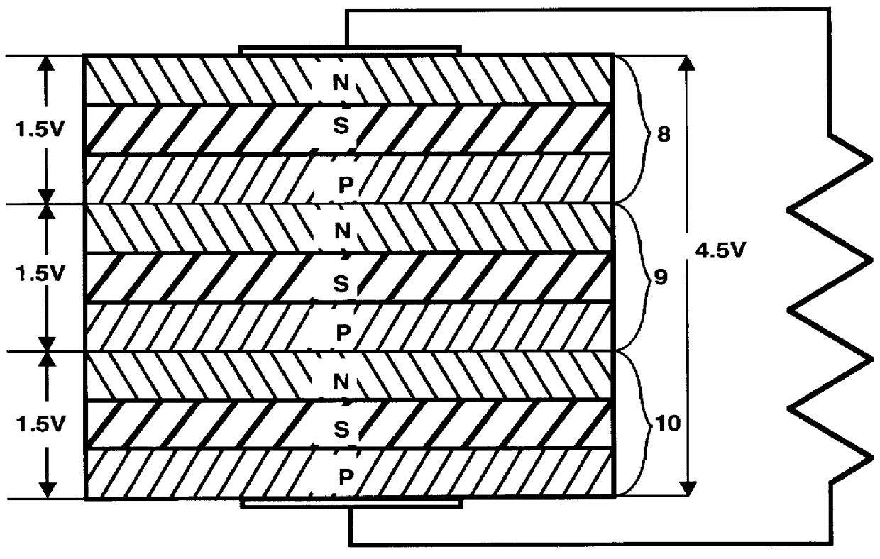
The present invention uniquely combines the formation by a radioactive flux of ions in an ionizable medium within an electric field with the storage capacity of a thin-film capacitor element to provide a power source having a useful life measured in years, without the need for recharging. An isotopic electric converter constructed according to the principles of the present invention is essentially a constant-voltage generator with an internal impedance determined by the materials of construction. The power cell of the present invention converts the energy of radioactive decay products directly to electrical energy, and provides an available lifetime for power generation that is a function of the radioactive half-life of the material utilized.
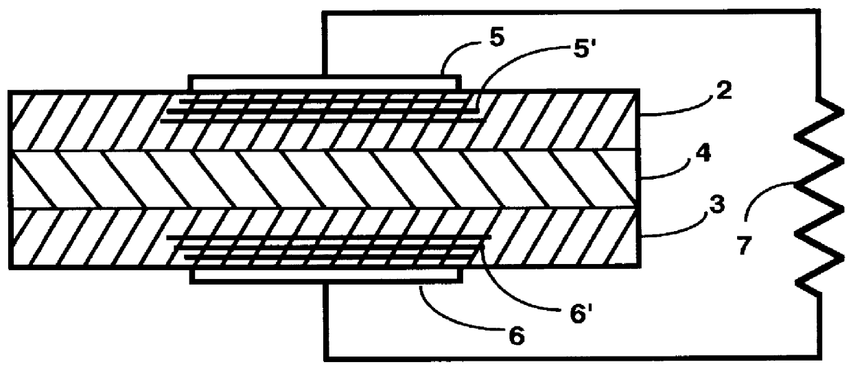
The space between the regions 2 and 3 is filled with an ionizable semiconductor 4, which, when ionized, provides a conducting medium between the regions 2 and 3. The electrons and holes in the ionized semiconductor 4 migrate to the positively and negatively charged regions, respectively, thereby providing a current flow when an external circuit through load 7 is connected. The semiconductor 4 may be ionized by any suitable well-known method. Electron-hole recombination in the semiconductor 4 does occur so that separation of regions 2 and 3 must be selected at an optimum width to minimize recombination. Preferably, electrodes 5 and 6 are about 300 nm apart. Electron-hole separation and reduction of recombination may be enhanced by the imposition of a magnetic field with the magnetic flux perpendicular to the regions 2 and 3 surfaces.

Problems solved by technology

Other technologies have been explored, including the pn-junction type converter, and are currently under development by several laboratories, but none of the other technologies have yet seen substantial commercial application.
This device is relatively bulky and inefficient due to the metallic electrodes, and recombination within the semiconductor, together with space charge effects, limit its efficiency, resulting in relatively low power density.
However, all the problems inherent to the RTG design are still present, namely, the apparatus is large and massive and works with great inefficiency, and substantial shielding is required because the radioisotope employed is of great health risk.
This type of apparatus does exhibit a multiplication factor, but is limited by the use of the dielectric material to pulsed operation.
Recombination within the secondary emitter limits the efficiency of the apparatus.
Although these types of cells are fairly reliable, their efficiency is severely limited by the indirect method used for the energy conversion.
This type of cell lacks stability, however, and soon loses its powergenerating effectiveness, which loss is attributed to dangling-bond degradation.
Also, their space charge effects, as well as reverse leakage currents, will limit their efficiency for power generation.
However, the problems inherent to the pn-junction type of cell are that the junction is a fragile crystalline structure and constant bombardment of beta particles causes material degradation effects.
The degradation effects destroy the junction and limit its useful life, and also limit the upper power availability of this type of apparatus.
Annealing or hardening of the junction has been employed to reduce the effects and provide greater operating life from such cells, but the problem of material degradation still remains.
Each of the above-cited U.S. patents discloses apparatus and means for converting radioactive decay energy into electricity, yet none of the designs has seen substantial commercial application due to the shortcomings of each design.
Since that decay energy is fairly constant, the electrical output from such an apparatus is fairly constant and no means is provided for increased power demand for peak operations, such as the start-up of the electrical load.

Method used


Image

  • Layered metal foil semiconductor power device
  • Layered metal foil semiconductor power device
  • Layered metal foil semiconductor power device

Examples


Embodiment Construction

The entrapment of tritium is particularly apt in this application as it is readily substituted for the hydrogen present in hydrogenated amorphous semiconductors with good intrinsic electronic properties. Radioisotopes other than tritium, may also be used as a source of energetic electrons as well as other forms of energetic nuclear radiation such as krypton-85, for example. All films were deposited using an ion-sputtering system.

Hydrogenation of amorphous silicon is essential as it serves to significantly reduce the defect nature of amorphous silicon by terminating a majority of the defective silicon bonds. Typically 10 to 25 atomic percent hydrogen is incorporated into amorphous silicon hydride to obtain a material with good semiconductor properties. The hydrogen is bonded to silicon and can be chemically stable to temperatures of 300 degrees C. Tritiated amorphous silicon can be deposited in the form of small and large area thin films onto a wide variety of substrates, electricall...


PUM


Abstract

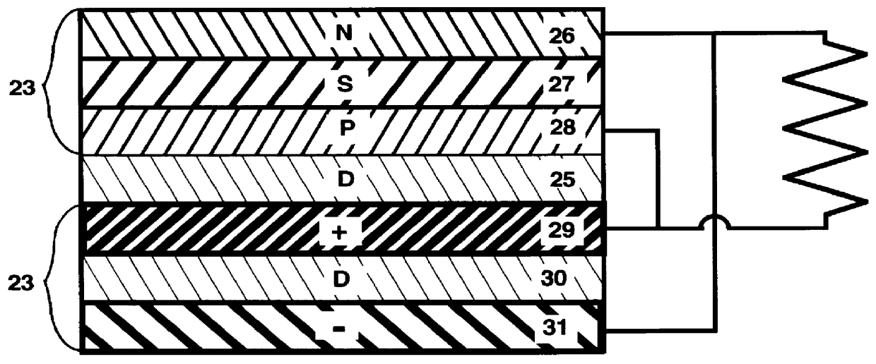
The present invention is a power cell for directly converting ionizing radiation into electrical energy. The invented isotopic electric converter provides an electrical power source that includes an electronegative material layered in a semiconductor, to form a first region that has a high density of conduction electrons, and an electropositive material also layered in the semiconductor material to form a second region with a high density of holes. Said N-layers region and P-layers region are separated by a neutral zone of semiconductor material doped with a radioactive isotope, such as, but not limited to, tritium. No junction is formed between the N and P layers regions. Rather, the potential gradient across the neutral zone is provided by the difference between the work functions of the electronegative and electropositive electrodes. Electrical contacts are affixed to the respective regions of the first and second type conductivity which become the anode and cathode of the cell, respectively. Beta particles emitted by the tritium generate electron-hole pairs within the neutral zone, which are swept away by the potential gradient between the first and second regions, thereby producing an electric current.

Description

1. Field of the Invention.The present invention generally relates to apparatus for the direct conversion of radioactive decay energy to electrical energy without going through a thermal cycle, and more particularly, it relates to semiconductor power cells which convert ionizing radiation directly into electrical energy.2. Related ArtThe decay of radioactive materials produces electrically charged particles such as alpha and beta particles as well as photons such as gamma rays. As with other nuclear processes, the charge scale of these types of radiation is millions of times greater than in non-nuclear processes.For example, isotope Americium-241 has a half-life of 458 years and produces alpha decay which can introduce 5.5 million electron volts (MeV) into a typical ionizable material. On the average, only 3.6 electron volts (eV) are necessary to produce one electron-hole pair within the typical semiconductor material. Thus, for every alpha particle traveling through a semiconductor ...

Claims


Application Information

Patent Timeline
IPC IPC(8): H01M14/00
CPCG21H1/06
Inventor BROWN, PAUL M.
Owner BROWN PAUL M
Learn More