Photoelectric conversion apparatus

a technology of conversion apparatus and photoelectric field, which is applied in the direction of superconductor devices, radiation controlled devices, transistors, etc., can solve the problems of limited constituting materials and formation methods, inconvenient use, and inconvenient operation

Inactive Publication Date: 2000-10-03
CANON KK
View PDF13 Cites 32 Cited by
  • Summary
  • Abstract
  • Description
  • Claims
  • Application Information

AI Technical Summary

Problems solved by technology

However, the conventional structure suffers from two drawbacks.
Although the above-mentioned element structure is one means for realizing a low-noise APD, various limitations are exerted in practice upon formation of an element having such a structure.
In order to obtain an element having stepback structure layers which can promote ionization by only changing a composition ratio of the constituting materials, constituting materials and a formation method are limited.
However, Ga, As, Hg, Cd, and the like used herein are materials posing a lot of problems in industrial use since they have high toxicity, and are rare and expensive elements.
However, the MBE requires an ultra high vacuum, has a low growth rate of a semiconductor, and is not suitable for a large-area structure, thus disturbing mass-production.
Therefore, when such a light-receiving element is stacked on a semiconductor device on which integrated circuits, and the like have already been formed, the existing semiconductor device may be damaged.
As a result, the band gap of an actually formed APD is limited.
In this element, a leaking current (dark current) signal which is generated when no light is radiated tends to be generated, and increases noise components.
As a result, a low-noise element cannot be obtained, thus posing a serious problem.
However, any conscious and sufficient consideration is not made in this respect, and this effect is not satisfactory.
However, this element is too narrow in minimum band gap to suppress the thermally generated carriers.
A semiconductor light-receiving element having such a band gap is suitable for receiving light within a wavelength range of 1.0 .mu.m to 1.6 .mu.m, but is not suitable for light-receiving elements in other wavelength ranges, e.g., for a visible light light-receiving element, resulting in a limited application field.
Thus, the second materials are not promising ones.
(1) Since incident light is absorbed by the p-type semiconductor layer and the multiplication layers, a multiplication ratio is changed depending on an incident wavelength of light, and is not suitable for a reading element.
(2) Since light absorption layers and multiplication layers have small forbidden bandwidths, a dark current during an operation is high, and noise is large.
(3) Since the element aims at optical communication, materials are limited, light to be coped with falls within a range of about 800 to 1,600 nm, and light in other wavelength ranges such as visible light cannot be coped with.
The technical problems upon manufacture of the element are as follows:
(1) In order to form a stepback structure using compound semiconductors, it is difficult to modulate compositions, and magnitudes of .DELTA.Ec and .DELTA.Ev are limited, thus restricting a low-noise structure.
(2) Since compound semiconductors belonging Groups III-V, II-IV, and the like are used as materials, there are problems as industrial materials such as toxicity and material costs.
(3) A formation method of compound semiconductors suffers from various problems. For example, an ultra high vacuum must be set, film formation must be performed at high temperatures (about 500 to 650.degree. C.), a large-area structure is difficult to attain, etc. Therefore, this method is not suitable for a manufacturing method of a reading element.

Method used


Image

  • Photoelectric conversion apparatus
  • Photoelectric conversion apparatus
  • Photoelectric conversion apparatus

Examples


embodiments

Embodiment 1

Embodiments of a photoelectric conversion apparatus of the present invention will be described hereinafter.

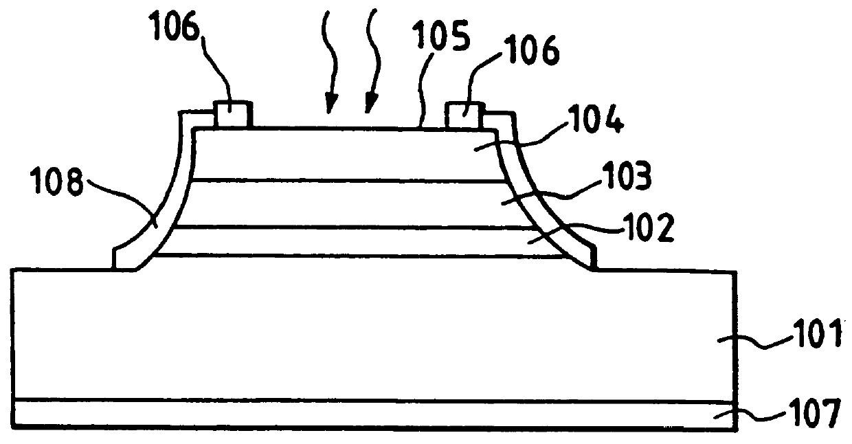
FIG. 7A is a schematic sectional view showing an embodiment of a photoelectric conversion element as a characteristic feature of the present invention.

Note that the size of the element and the thicknesses of the respective layers are exaggerated to some extent since constituting elements of the element of this embodiment are illustrated clearly.

The element shown in FIG. 7A comprises ohmic-contact layers for applying a voltage to the element or extracting signals therefrom, i.e., so-called electrodes 1 and 6, a blocking layer (electric charge injection blocking layer) 2 for blocking injection of carriers from the electrode 1, a blocking layer 5 for blocking injection of carriers from the electrode 6, a light-receiving layer 3, sandwiched between these blocking layers, for absorbing light incident on the element from the electrode 1 side, and generating photocarriers ...

embodiment 2

The second embodiment corresponding to a case wherein spatial electric charges caused by impurity doping, a deflect level, an interface level, and the like are present in the respective layers constituting the avalanche region (multiplication layer) 4 shown in FIG. 7A will be described below. In this case, an electric field generated in each layer upon application of a bias voltage for depleting the avalanche region 4 depends on a dielectric constant and a spatial electric charge amount of each layer.

FIG. 8 shows an energy band structure of a portion of the avalanche region when each layer of the avalanche region of the semiconductor light-receiving element having the element structure shown in FIG. 7A has spatial electric charges.

The structure shown in FIG. 8 is constituted by layers 31, 33, and 35 each having a layer thickness l.sub.1, and a constant total electric charge density .rho..sub.1, which is constant regardless of positions in the layer, and a dielectric constant .epsilo...

embodiment 3

The third embodiment corresponding to a case wherein a layer having a given dielectric constant and a layer having a dielectric constant smaller than the given dielectric constant have a band gap difference and an electron affinity difference in the layers constituting the avalanche region of the semiconductor light-receiving element having the element structure shown in FIG. 7A will be described below. In general, a material having a small dielectric constant tends to have a large band gap. Thus, when materials having desired dielectric constants are selected from a wide range of materials to constitute a plurality of dielectric constant change layers constituting the avalanche region, a band gap difference and an electron affinity difference often occur. For example, as combinations of materials having large and small dielectric constants, which constitute the avalanche region, silicon and a silicon oxide, silicon and a silicon nitride, silicon and a silicon carbide alloy, and the...


PUM


Abstract

A photoelectric conversion apparatus of this invention has a high sensitivity and low noise, and can be formed to have a large area at a relatively low temperature since it has a light absorption layer (310), formed of a non-monocrystalline material, for absorbing light and generating photocarriers, and a multiplication layer (301, 303, 305, 307, 309) for multiplying the photocarriers generated by the light absorption layer.

Description

1. Technical FieldThe present invention relates to a photoelectric conversion apparatus and, more particularly, to a photoelectric conversion apparatus utilizing an avalanche effect for amplifying optically generated carriers by impact ionization.In particular, the present invention relates to a low-noise photoelectric conversion apparatus suitably used in a photometric sensor for a camera, or an image sensor for an image reading apparatus such as a facsimile system, a copying machine, or the like, or a light-receiving sensor in an optical communication apparatus, or the like.2. Related Background ArtIn information transmission techniques in a video information system, optical communication, and other industrial and commercial fields, which utilize light as a medium of an information signal, a semiconductor light-receiving element for converting a light signal into an electrical signal is one of the most important and basic constituting elements, and a large number of elements have ...

Claims


Application Information

Patent Timeline
Patent Type & Authority Patents(United States)
IPC IPC(8): H01L29/06H01L29/02H01L31/102H01L31/075H01L31/06H01L31/105H01L39/00H01L27/146H01L31/107
CPCH01L27/14609H01L31/1075H01L27/14681H01L31/035245Y02E10/548
Inventor SUGAWA, SHIGETOSHIGOFUKU, IHACHIROOHMI, KAZUAKIOSADA, YOSHIYUKIYAMANOBE, MASATO
Owner CANON KK
Why Eureka
Try Eureka