Tool tip and bonding tool comprising the tool tip and control method for the bonding tool

a technology of bonding tool and control method, which is applied in the direction of natural mineral layered products, record information storage, water-setting substance layered products, etc., can solve the problems of diamond film distortion, difficult to reduce the time required for single bonding of semiconductor chips, and inferior heat respons

Inactive Publication Date: 2001-08-07
SUMITOMO ELECTRIC IND LTD
View PDF12 Cites 21 Cited by
  • Summary
  • Abstract
  • Description
  • Claims
  • Application Information

AI Technical Summary

Problems solved by technology

In case of the pulse heat system, however, there is such a problem that heat response is inferior as compared with a tool tip consisting of a pure metal such as nichrome, molybdenum, inconel or stainless steel to which no diamond film is stuck since temperature rise of the diamond film stuck to the pressing surface on the forward end results from heat transfer from a tool base material.
Therefore, it is difficult to reduce the time required for single bonding of the semiconductor chip.
Hence, there are such problems that distortion takes place in the diamond film due to difference of thermal expansion in temperature rise and flatness of the pressing surface on the forward end of the tool tip is hard to ensure.
According to the technique disclosed in the aforementioned Japanese Patent Laying-Open Gazette No. 5-226421, there are such problems that the cost for the tool tip increases and the tool tip is easy to break in handling thereof since the material used for the tool tip itself is diamond.
Further, there are such problems that a step of dissolving/removing SiO.sub.2 is required after forming the conductive diamond film and the tool ti

Method used


Image

  • Tool tip and bonding tool comprising the tool tip and control method for the bonding tool
  • Tool tip and bonding tool comprising the tool tip and control method for the bonding tool
  • Tool tip and bonding tool comprising the tool tip and control method for the bonding tool

Examples


concrete example 1

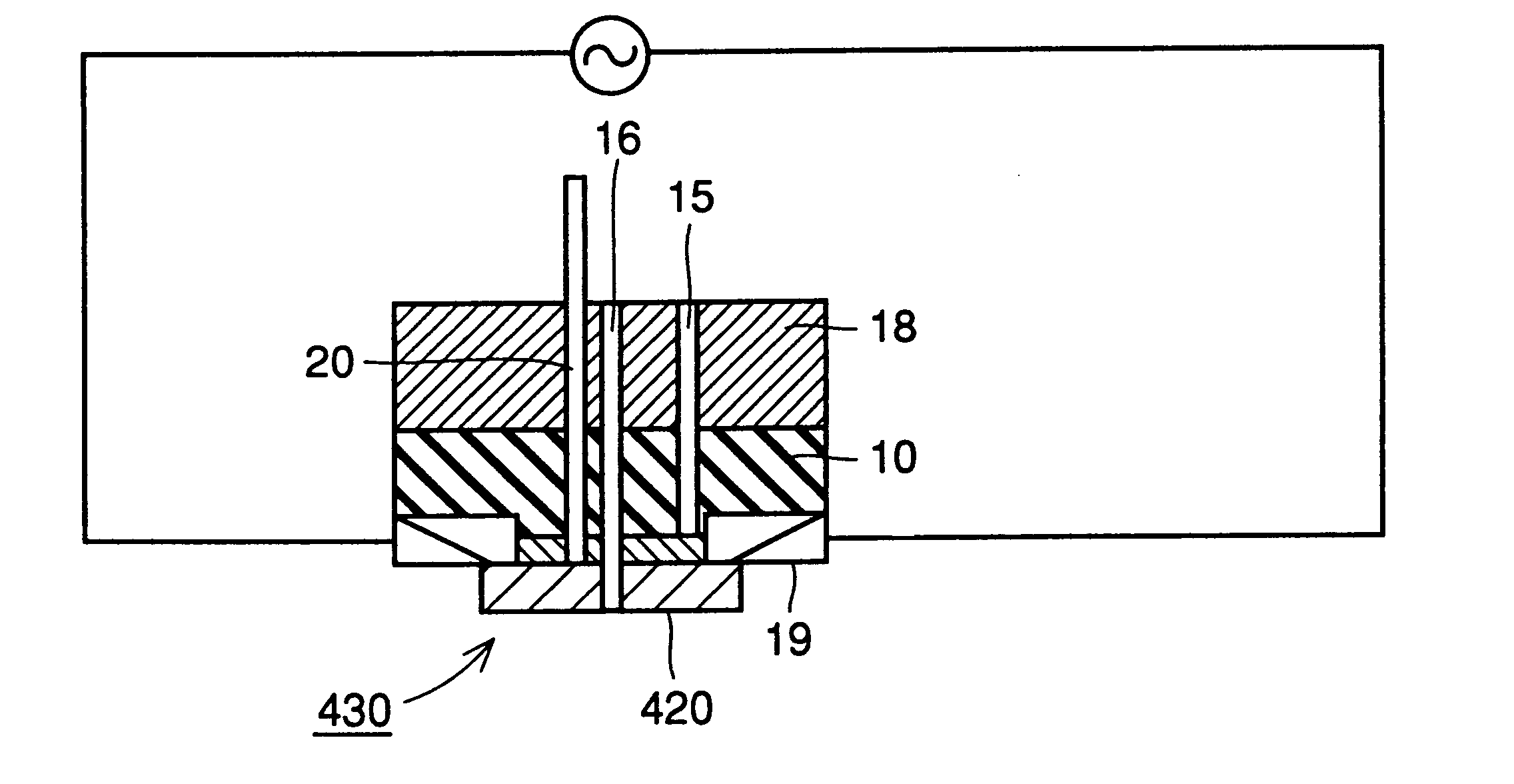
First, the structure of a tool tip 400 in this Concrete Example 1 is described with reference to FIG. 7A to FIG. 7C. A conductive polycrystalline diamond film 1 of about 10 .mu.m in film thickness and 8.times.10.sup.-3 .OMEGA.cm in specific resistance to which boron is added as an impurity is deposited by a vapor-phase synthetic method on a surface of 20 mm.times.20 mm of an SiC substrate 2 of 20 mm.times.20 mm.times.5 mm having one suction through hole 5 of about 1 mm in diameter on its central portion. Thereafter an insulating diamond film 6 is further deposited by 50 .mu.m on the conductive polycrystalline diamond film 1.

Both of the conductive polycrystalline diamond film 1 and the insulating diamond film 6 are formed by microwave plasma CVD with methane and hydrogen as gas.

The gas flow rates in this film formation are 5 sccm for methane and 500 sccm for hydrogen, and diborane of B / C=20000 ppm with respect to methane was added to the material gas during film formation of the cond...

concrete example 2

Concrete Example 2 is now described.

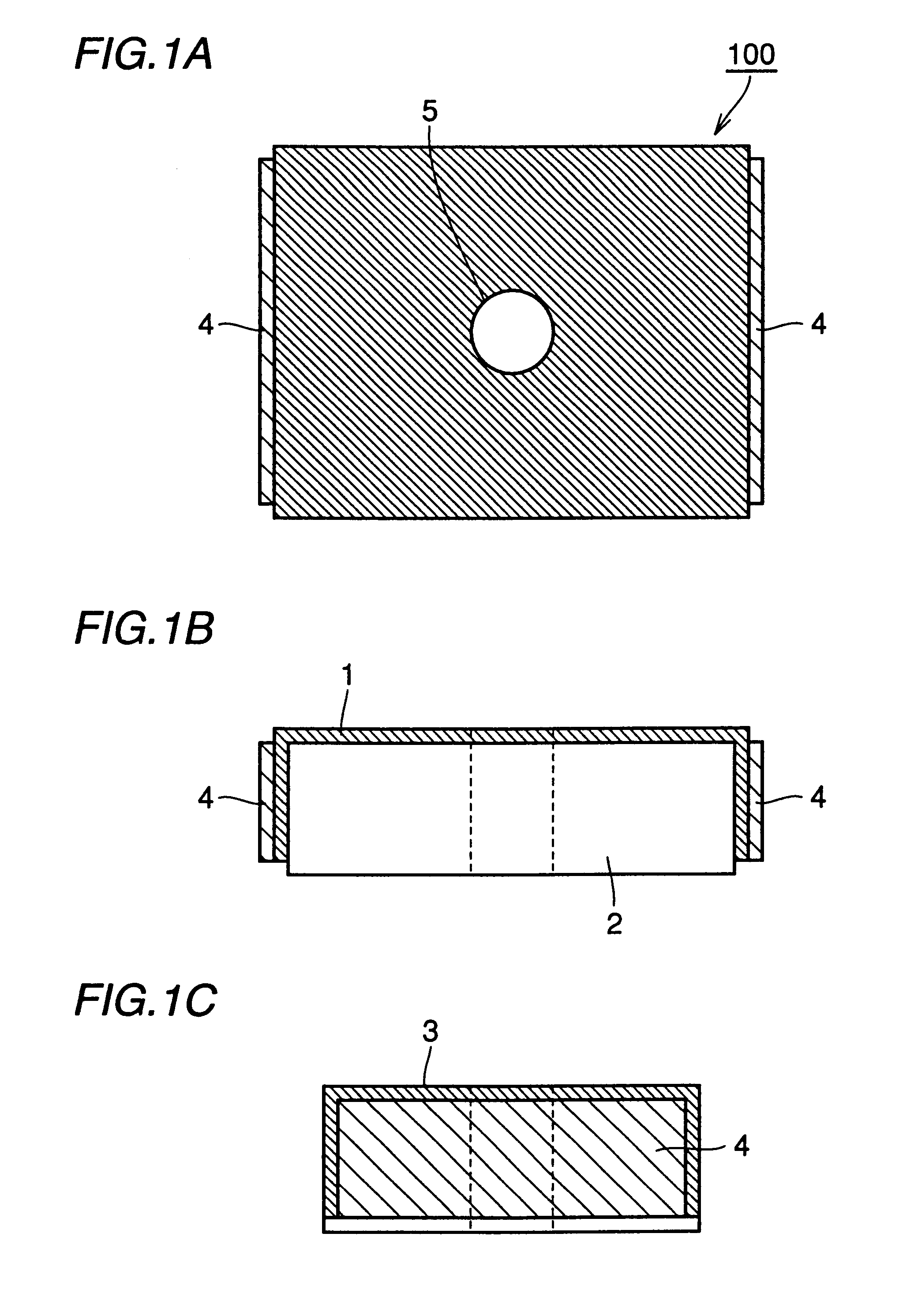
Referring to FIG. 13A to FIG. 13C, a conductive polycrystalline diamond film 1 of 8 .mu.m in film thickness and 8.times.10.sup.-3 .OMEGA.cm in specific resistance to which boron was added as an impurity was deposited by a vapor-phase synthetic method on a substrate 2 consisting of insulating polycrystalline diamond of 12 mm.times.12 mm.times.0.3 mm in a tool tip 420 in this Concrete Example 2.

As to growth of a boron-added layer, film formation was performed by thermal filament CVD with methane, hydrogen and trimethyl boron of 5000 ppm with respect to methane as material gas.

When a conductive polycrystalline diamond film synthesized by the same conditions was analyzed by SIMS, it was found that boron was contained therein by 800 appm.

After formation of the conductive polycrystalline diamond film 1, a suction through hole 5 of about 1 mm in diameter was formed on a central portion of the substrate 2 by excimer laser beam machining.

After forming the ...

concrete example 3

Concrete Example 3 is now described.

With reference to FIG. 17A to FIG. 17C, the structure of a tool tip 440 in this Concrete Example is described. A conductive polycrystalline diamond film 1 of about 10 .mu.m in film thickness and 1.times.10.sub.3 .OMEGA.cm in specific resistance containing a crystal fault synthesized and obtained with high methane concentration is deposited on a surface of 20.times.20 mm of an SiC substrate 2 of 20 mm.times.20 mm.times.3 mm having one suction through hole 5 of about 1 mm in diameter on its central portion.

Thereafter an insulating diamond film 6 is deposited on a surface opposite to the conductive polycrystalline diamond film 1 by about 50 .mu.m. Both of the conductive polycrystalline diamond film 1 and the insulating diamond film 6 were synthesized by microwave plasma CVD with methane and hydrogen as material gas. The methane flow rate during film formation of the conductive polycrystalline diamond film 1 was 50 sccm, and that of hydrogen was 500 s...


PUM

PropertyMeasurementUnit
Fractionaaaaaaaaaa
Fractionaaaaaaaaaa
Temperatureaaaaaaaaaa

Abstract

A conductive polycrystalline diamond film having specific resistance of at least 1x10⁻⁴ OMEGAcm and less than 1x10³ OMEGAcm, whose film thickness is in the range of at least 0.1 mum and not more than 500 mum, is film-formed by vapor-phase synthesis on a surface employed for pressure bonding, a surface opposite to this surface or at least two side surfaces intersecting with these surfaces on a substrate of a bonding tool tip that is applicable for bonding and packaging a semiconductor chip.

Description

The present invention relates to a tool tip and a bonding tool comprising the tool tip and a control method for the bonding tool, and more specifically, it relates to improvements of structures of a tool tip employed in a step of bonding electrodes of a semiconductor chip to lead wires or external terminals and a bonding tool comprising the tool tip and a control method for the bonding tool.BACKGROUND TECHNIQUEGenerally in packaging of a semiconductor chip, it is necessary to carry out a step of connecting electrodes formed on the semiconductor chip and external terminals or lead wires with each other. In this step, the electrodes of the semiconductor chip and the external terminals or the like are connected with each other with interposition of a brazing filler metal of gold or tin, an anisotropic conductive film or resin such as a conductive adhesive.At this time, a tool tip is employed for locating and pressing the semiconductor chip on and against prescribed positions of the ext...

Claims


Application Information

Patent Timeline
IPC IPC(8): B23K3/02H01L21/683H01L21/67H01L21/68B23K26/38B23K26/40H01L21/00
CPCB23K26/381B23K26/408H01L21/67138B23K26/4005B23K26/4025B23K26/4095B23K2201/20Y10T428/30Y10T428/24917Y10T428/24802Y10T428/24926Y10T428/24628Y10T428/24355Y10T428/26B23K26/40B23K26/382B23K2101/20B23K2101/35B23K2103/50B23K2103/52H01L21/68
Inventor YAMAMOTO, KATSUKOIGUCHI, TAKAHISAKUMAZAWA, YOSHIAKITANAKA, KATSUYUKISHIOMI, HIROMUTSUNO, TAKASHIFUJIMORI, NAOJI
Owner SUMITOMO ELECTRIC IND LTD
Why Eureka
Try Eureka