
Process for producing heteropitaxial diamond layers on Si-substrates

a technology of si-substrates and diamond layers, applied in the direction of crystal growth process, chemical vapor deposition coating, coating, etc., can solve the problem of low surface energy

Inactive Publication Date: 2001-08-14
DAIMLER BENZ AG
View PDF12 Cites 11 Cited by
  • Summary
  • Abstract
  • Description
  • Claims
  • Application Information

AI Technical Summary

Benefits of technology

3. The method according to the invention makes it possible to perform the surface cleaning of substrates, nucleation and the growth of the diamond layers in a single process.
This opens the door to completely new applications, such as the use as heat-conducting, insulating layers (power semi-conductors, laser diodes, etc.) or as a heat-conducting layer with a high electrical resistance and a high disruptive field for cooling semiconductor components. Other possible uses are as optical windows with a high mechanical stability and low absorption as well as as an active semiconductor material in electronic components and as a piezoresistive sensor or thermistor.

Problems solved by technology

As compared with diamond, silicon has widely differing lattice parameters and a low surface energy, it is not possible under normal conditions to form a high nucleus density on not pretreated silicon and thereby achieve diamond deposition.

Method used


Image

  • Process for producing heteropitaxial diamond layers on Si-substrates
  • Process for producing heteropitaxial diamond layers on Si-substrates
  • Process for producing heteropitaxial diamond layers on Si-substrates

Examples


Embodiment Construction

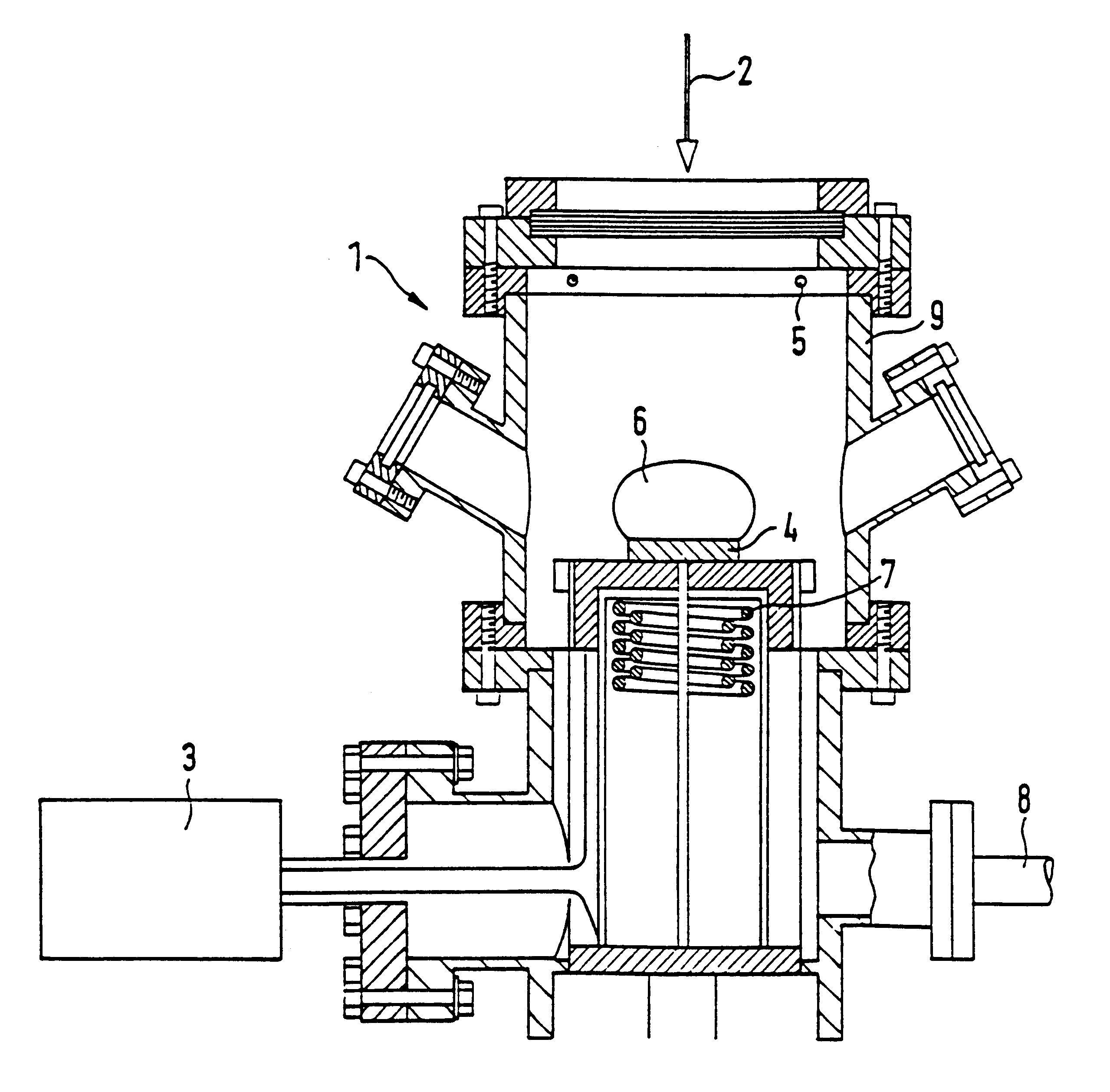
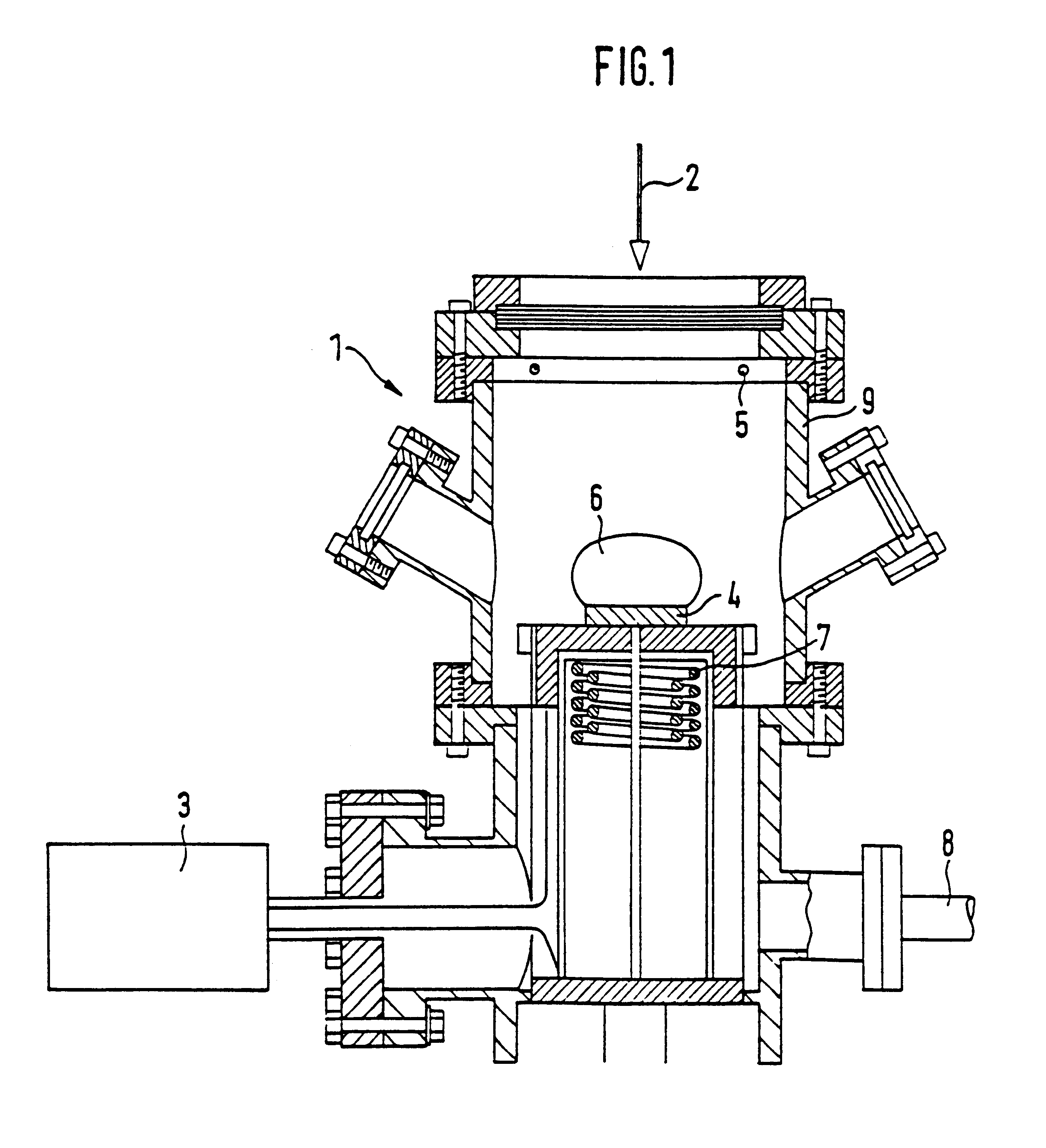
FIG. 1 shows an exemplified test setup. Use is made in the present embodiment of a MWPCVD unit 1, which has a microwave generator with an adjustable microwave power of up to 1.5 kW for producing a microwave 2. According to the invention the MWPCVD unit is provided with a d.c. bias voltage supply 3, which is adjustable up to .+-.300 V.

In each test, prior to the deposition experiment, a (100) silicon substrate 4 was cleaned in an acetone ultrasonic bath. After positioning the substrate 4 in the reactor 1 the vacuum chamber is evacuated to 10.sup.-2 mbar and the substrate heated. The process gases are then supplied via the gas supply 5 and the plasma 6 is ignited. The reactor is heated by means of the heating system 7. The vacuum is produced by means of the pump connection 8. A water cooling system 9 is provided for cooling purposes.

The layer production method takes place according to the invention in the three following stages:

1. plasma cleaning of the substrate surfaces,

2. diamond nu...


PUM

PropertyMeasurementUnit
Fractionaaaaaaaaaa
Fractionaaaaaaaaaa
Fractionaaaaaaaaaa

Abstract

The invention relates to a method for producing heteroepitaxial diamond layers on Si-substrates by means of CVD and standard process gases, in which (a) during the nucleation phase a negative bias voltage is applied to the Si-substrate and (b) following the nucleation phase diamond deposition takes place.

Description

BACKGROUND OF THE INVENTIONThe invention relates to a method for producing heteroepitaxial diamond layers from the vapor phase on a silicon substrate, as well as to layers produced by this method and the use thereof.As is known from M. W. Geis et al, IEEE Electron Device Letters EDL-8, 1987, 341 and M. W. Geis et al, J. Vac. Sci. Technol., A 6, 1988, 1953, as a result of its excellent physical properties such asband gap 5.5 eV hole mobility 1800 cm.sup.2 / V.sub.s electron mobility 2000 cm.sup.2 / V.sub.s electron saturation drift rate 2 .times. 10.sup.7 cm / s disruptive field 1 .times. 10.sup.7 V / cm thermal conductivity 20 W / cmK relative permativity 5.7diamond is an excellent material, which is suitable for high temperature, high frequency and high power semiconductor components.After Japanese scientists described at the beginning of the 1980's that diamond can be synthesized as a layer or coating from gaseous substances, numerous efforts were made throughout the world to find new app...

Claims


Application Information

Patent Timeline
IPC IPC(8): C23C16/02C23C16/26C30B25/10C23C16/27H01L21/205H01L21/02G01L9/04C30B25/02G01D21/00G01K7/22G01L9/00H01C7/04H01L21/00
CPCC23C16/0209C23C16/274C30B25/105H01L21/02661H01L21/02381H01L21/02527H01L21/0262C30B29/04
Inventor KLAGES, CLAUS-PETERJIANG, XINFUSSER, HANS-JURGENHARTWEG, MARTINZACHAI, REINHARDROSLER, MANFRED
Owner DAIMLER BENZ AG
Learn More