Seamless, maskless lithography system using spatial light modulator

a lithography system and mask technology, applied in the field of maskless, maskless lithography system using spatial light modulator, can solve the problems of significant fraction of the cost of integrated circuit (ic) manufacturing, significant drag on the time required to build electronic module prototypes, and the cost of maintaining an array, so as to eliminate the need for masks and high exposure throughput , the effect of high resolution

Inactive Publication Date: 2001-11-06
ANVIK CORP
View PDF12 Cites 439 Cited by
  • Summary
  • Abstract
  • Description
  • Claims
  • Application Information

AI Technical Summary

Problems solved by technology

The process of designing and constructing a mask places a significant drag on the time required to build electronic module prototypes.
The time required for switching and aligning masks as well as the expense of maintaining an array of masks for the production of a single electronic module represents a significant fraction of the cost of integrated circuit (IC) manufacturing.
Good contact is difficult to produce over a large area.
Poor contact, or a proximity gap, results in limited resolution.
Frequent contact between the mask and the board causes generation of defects on the board which results in lower yields and causes reduction of the mask life, which leads to higher overall costs.
In addition, variations in the gap cause feature size errors.
The technology to manufacture the masks themselves is a real impediment to manufacturing large-area FPDs.
All projection printing systems suffer from the limitation that there exists a trade-off between the resolution and the maximum image field size of the projection lens.
For larger areas the total imaging field must be broken up into segments which then must be imaged one at a time in a step-and-repeat fashion, thereby limiting the available throughput.
Generally, systems with larger reduction ratios provide higher resolution, but also lower throughput.
As described above for contact printing systems, masking technology leads to many problems: use of masks does not allow for rapid prototyping of electronic modules; a different mask is required for subsequent layers of an electronic module, adding considerably to the expense of manufacturing; and the production capability of large-area masks does not meet all the current industry requirements for precision and accuracy at low cost and on fast schedules.
In addition, conventional projection imaging systems, due to fundamental lens-design considerations governing their performance, are forced to make a trade-off between resolution and image field size.
Step-and-repeat imaging also leads to higher costs due to the requirement of several masks and the errors introduced in stitching the different fields together.
Thus, although direct-write systems avoid the problems associated with using masks, they are extremely slow because transfer of the pattern information takes place in a bit-by-bit serial mode.
Due to the large number of pixels (.about.10.sup.8 -10.sup.10) that must be written on an electronic module, typical processing times with such systems are unacceptably long for cost-effective volume manufacturing.
From the above descriptions, it is clear that existing technologies for microelectronic patterning suffer from critical limitations.
There are several systems that are capable of producing images utilizing deformable micromirror devices, but none provide a seamless pattern on a large substrate.
There is no scanning ability and no system for image error correction.
There are exposure systems that are capable of scanning, but with limitations.
Although there is some scanning capability, there are no provisions for seamless scanning or error correction.

Method used


Image

  • Seamless, maskless lithography system using spatial light modulator
  • Seamless, maskless lithography system using spatial light modulator
  • Seamless, maskless lithography system using spatial light modulator

Examples


Embodiment Construction

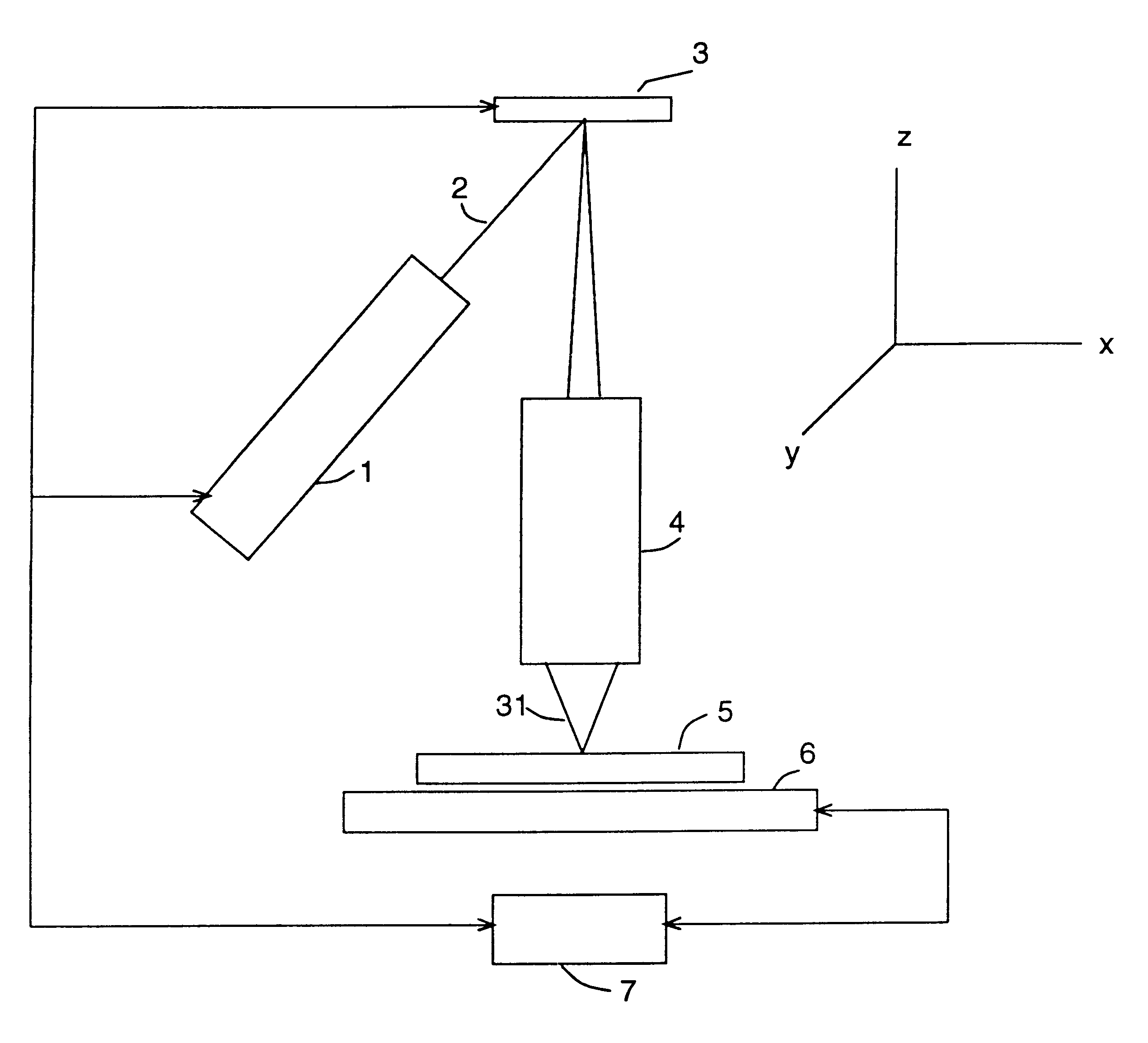
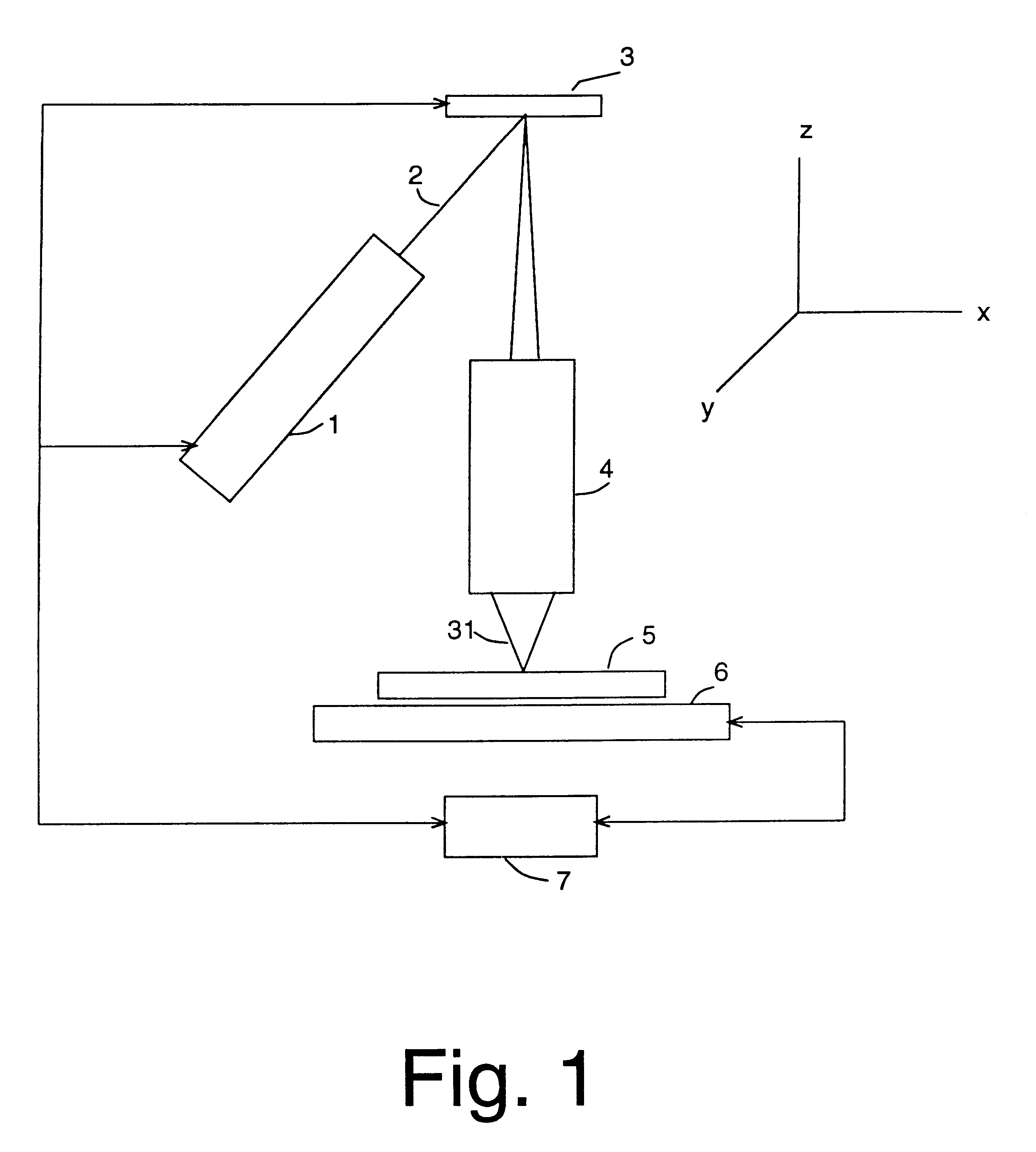
FIG. 1 is a schematic illustration of a preferred embodiment of the maskless lithography system. The illumination for exposure is provided by a radiation source 1 with output beam 2. The output beam 2 then illuminates a spatial light modulator, shown in FIG. 1 as a deformable micromirror device (DMD) 3, which is an array of micromirrors on a chip with electronic logic, memory and control that enable the individual mirrors to tilt in different directions for selective reflection or deflection of individual pixels. The illuminated DMD pixels which are reflective are imaged by a projection lens 4 onto a substrate 5 which rests on a scanning stage 6. The reduction power of the lens determines the resolution of the invention for a particular DMD pixel size. For example, a lens with reduction of 10:1 will produce a pixel size on the substrate which is one tenth the size of an individual micromirror.

The substrate is scanned as shown in FIG. 1 along, say, the y-axis. Simultaneously, control...


PUM

PropertyMeasurementUnit
diameteraaaaaaaaaa
diameteraaaaaaaaaa
diameteraaaaaaaaaa

Abstract

The invention is a seamless projection lithography system that eliminates the need for masks through the use of a programmable Spatial Light Modulator (SLM) with high parallel processing power. Illuminating the SLM with a radiation source (1), which while preferably a pulsed laser may be a shuttered lamp or multiple lasers with alternating synchronization, provides a patterning image of many pixels via a projection system (4) onto a substrate (5). The preferred SLM is a Deformable Micromirror Device (3) for reflective pixel selection using a synchronized pulse laser. An alternative SLM is a Liquid Crystal Light Valve (LCLV) (45) for pass-through pixel selection. Electronic programming enables pixel selection control for error correction of faulty pixel elements. Pixel selection control also provides for negative and positive imaging and for complementary overlapping polygon development for seamless uniform dosage. The invention provides seamless scanning by complementary overlapping scans to equalize radiation dosage, to expose a pattern on a large area substrate (5). The invention is suitable for rapid prototyping, flexible manufacturing, and even mask making.

Description

This invention relates to high-throughput lithography systems, and, more particularly, this invention relates to a maskless lithography system that provides large-area, seamless patterning using a spatial light modulator capable of being directly addressed by a control system.High-throughput lithography systems are advantageous in the manufacture of many electronic and opto-electronic products, which require fabrication of millions of microscopic structures on a single large substrate. Such structures may be in the form of active devices, such as the transistors in an electronic display or in a semiconductor integrated circuit, or may be in the form of passive patterns, such as the metal interconnect network in a multichip packaging module or in a printed circuit board. The large substrate can be a display panel, a silicon wafer, or a board. The pattern feature sizes in these diverse products, which shall be referred to as electronic modules, range from sub-micron for semiconductor ...

Claims


Application Information

Patent Timeline
Patent Type & Authority Patents(United States)
IPC IPC(8): G03F7/20
CPCG03F7/70291G03F7/70358G03F7/70475
Inventor JAIN, KANTIDUNN, THOMAS J.HOFFMAN, JEFFREY M
Owner ANVIK CORP
Why Eureka
Try Eureka