
Process for the manufacturing of oxide electrodes for ferroelectric capacitor

a ferroelectric capacitor and oxide electrode technology, applied in the field of electrochemical processes of ferroelectric capacitors, can solve the problems of dielectric capacitor deformation, poor processability, and impaired flatness of the lower electrode surface,

Inactive Publication Date: 2002-03-12
SONY CORP
View PDF15 Cites 34 Cited by
  • Summary
  • Abstract
  • Description
  • Claims
  • Application Information

AI Technical Summary

Benefits of technology

It is therefore an object of the present invention to provide an electrode for a capacitor, a dielectric capacitor of which is not degraded in characteristics when the electrode is exposed to a high-temperature atmosphere for a long period of time, said capacitor and a process for the manufacture of these.
In the present invention, the metal oxide layer is formed by oxidizing the surface of the metal layer on the basis of a diffusion-controlling reaction, so that the dense metal oxide layer of passivity can be formed under controlled conditions. Further, the metal oxide layer of at least one of the electrodes is formed so as to be present in an interface to the capacitor insulation layer, so that the capacitor is free from the impairment of flatness of the electrode surface caused by evaporation and / or re-oxidation when the electrode is exposed to a high-temperature atmosphere for a long period of time.
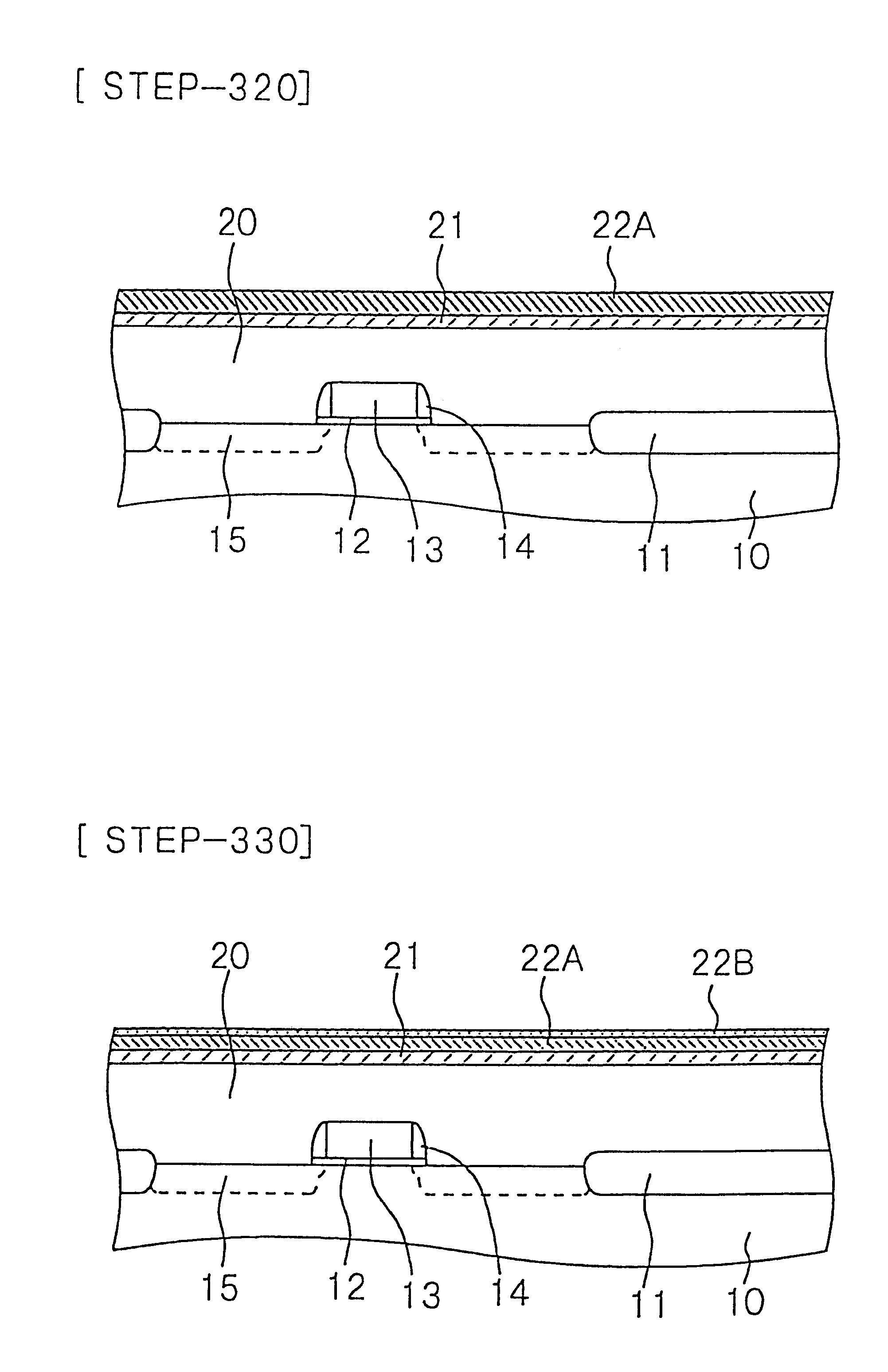
Thereafter, an insulating interlayer 20, for example, Of SiO.sub.2 is deposited on the entire surface of the semiconductor substrate 10. Then, a buffer layer 21 of Ti is deposited on the insulating interlayer 20 by sputtering, for improving the adhesion of a lower electrode layer to the insulating interlayer 20 and improving the crystallizability of the lower electrode layer. Then, a lower electrode layer 22A (corresponding to a metal layer) of Ru is formed (deposited) on the buffer layer 21 by sputtering (see FIG. 4A). The deposition conditions of the buffer layer 21 and the lower electrode layer 22A are as shown in Tables 2 and 3, in which "Distance from target" means a distance from a target to the semiconductor substrate.
The contact hole (contact plug) 19 can be also formed by filling, e.g., a metal wiring material of a refractory metal or metal silicide such as W, Ti, Pt, Pd, Cu, TiW, TiNW, WSi.sub.2, MoSi.sub.2 and the like in the opening portion 18 formed in the insulating interlayer 20. The top surface of the contact hole 19 may be located at the same level as that of the surface of the insulating interlayer 20, or the top surface of the contact hole 19 may extend on the surface of the insulating interlayer 20. The condition of filling the opening portion 18 with tungsten to form the contact hole 19 is as shown in the following Table 8. Before filling the opening portion 18 with tungsten, a Ti layer and a TiN layer are consecutively deposited on the insulating interlayer 20 including an inner surface of the opening portion 18, e.g., by magnetron sputtering. The Ti layer and the TiN layer are formed for obtaining a low ohmic contact resistance, preventing the occurrence of damage in the semiconductor substrate 10 in a blanket tungsten CVD method and improving the adhesion of tungsten.
A pedestal type RAM which is a kind of a stacked type RAM can be produced in the same manner as in Example 4. That is, the capacitor may have the form of a column. In the pedestal type RAM of which the partial cross section is schematically shown in FIG. 10, a lower electrode has the form of a column, and a capacitor insulation layer 23 has a structure in which it covers the surface of the lower electrode 22. In this structure, the effective area of the capacitor insulation layer 23 can be expanded, that is, the amount of stored charge of the capacitor can be increased.
In the present invention, the surface of a metal layer is oxidized on the basis of a diffusion-controlling reaction, to form a metal oxide layer, so that a dense metal oxide layer can be formed. Further, the metal oxide layer of at least one electrode is Ad formed so as to be positioned in an interface to a capacitor insulation layer, and therefore, the flatness of the electrode surface is not at all impaired by evaporation and / or re-oxidation even when the electrode is exposed to a high-temperature atmosphere for a long period of time. There can be therefore manufactured an electrode for a capacitor which can be suitably used in a semiconductor memory cell and is highly reliable, and said capacitor.

Problems solved by technology

Platinum is a stable material, while it has a defect that its processability is poor.
When these metals are used as a lower electrode in particular, the lower electrode is exposed to a high-temperature atmosphere for a long period of time and the flatness of the lower electrode surface is impaired by evaporation and / or re-oxidation of these materials.
As a result, there is caused a problem that the dielectric capacitor is degraded in characteristics.

Method used


Image

  • Process for the manufacturing of oxide electrodes for ferroelectric capacitor
  • Process for the manufacturing of oxide electrodes for ferroelectric capacitor
  • Process for the manufacturing of oxide electrodes for ferroelectric capacitor

Examples


example 2

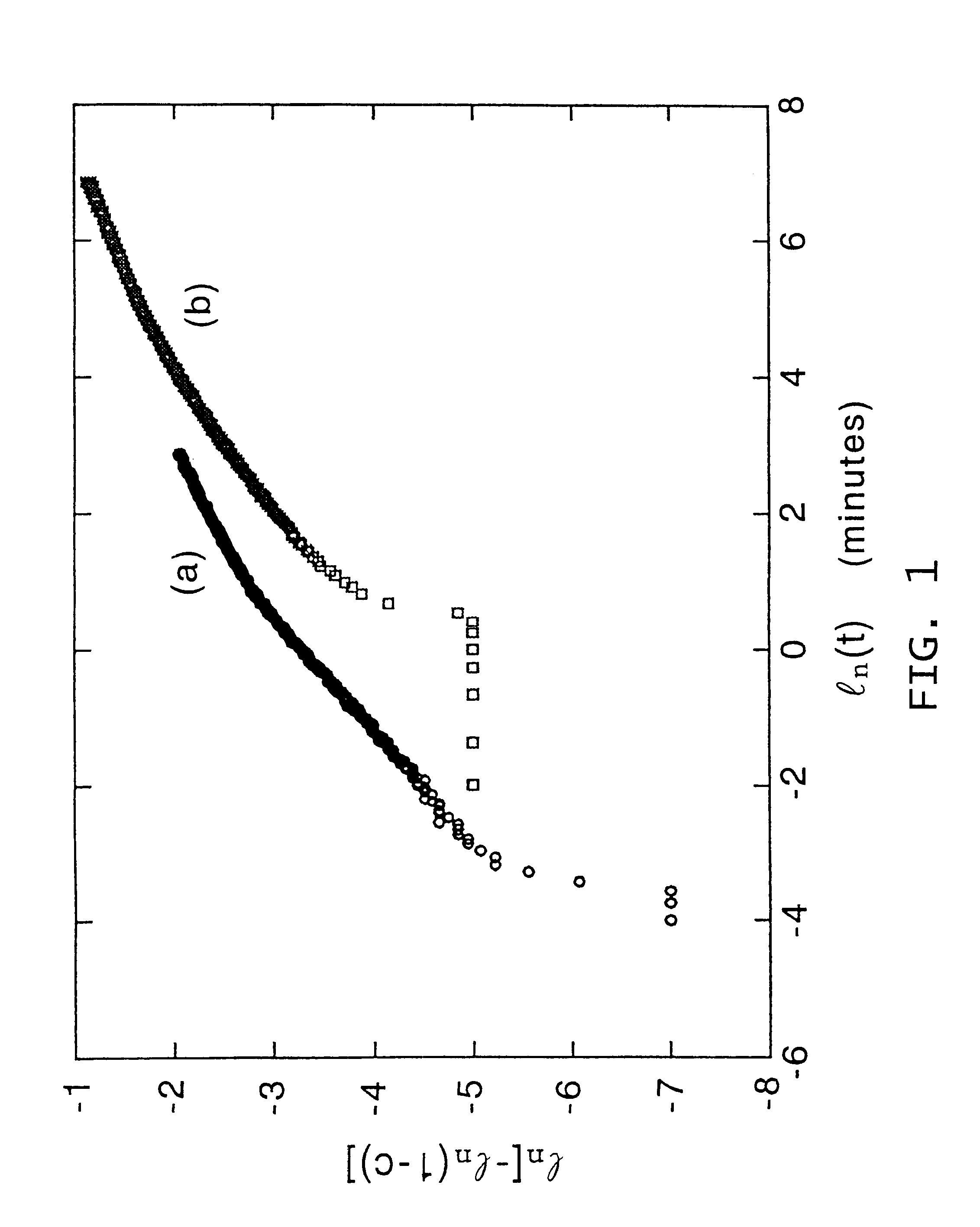
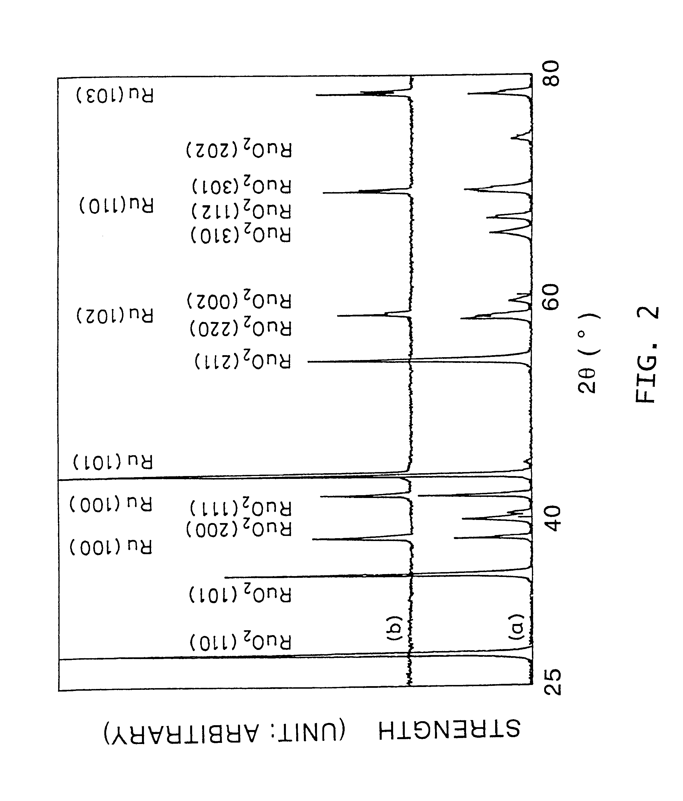
In Example 2, metal oxide layers were formed by heat-treating Ru metal single-crystal powders by holding them in (A) a 0.1 MPa oxygen atmosphere (oxygen gas concentration: 100% by volume), (B) a 0.02 MPa oxygen atmosphere (oxygen gas concentration 20% by volume, nitrogen gas concentration 80% by volume), and (C) a 0.004 MPa oxygen atmosphere (oxygen gas concentration: 4% by volume, nitrogen gas concentration: 96% by volume), at 1083 K for t minutes and thereby oxidizing the surface of each Ru metal single-crystal powder.

FIG. 3 shows the obtained relationship between t and C. In FIG. 3, the axis of ordinates shows ln{-ln(1-C)}, and the axis of abscissas shows ln(t) (unit: minute). In FIG. 3, "(a)" indicates data obtained when the oxygen atmosphere was set at 0.1 MPa, "(b)" indicates data obtained when the oxygen atmosphere was set at 0.02 MPa, and "(c)" 1 indicates data obtained when the oxygen atmosphere was set at 0.004 MPa. The data "(a)" to "(c)" in FIG. 3 show that graphs can ap...

example 3

In Example 3, an electrode for a capacitor for a semiconductor memory cell is prepared according to the process for the manufacture of an electrode for a capacitor and the process for the manufacture of the capacitor, provided by the present invention. The capacitor is composed of two electrodes and a capacitor insulation layer formed of a dielectric film (ferroelectrics film) sandwiched between the two electrodes. More specifically, the capacitor is composed of a lower electrode, a capacitor insulation layer formed of a ferroelectrics film formed on the lower electrode and an upper electrode formed on the capacitor insulation layer. In Example 3, a semiconductor memory cell is a so-called planar RAM, and the capacitor has the form of a flat plate. The process for the manufacture of an electrode for a capacitor and the process for the manufacture of the capacitor, provided by the present invention, will be explained with reference to FIGS. 4A to 7B hereinafter.

[Step-300]

First, a MOS...

example 4

In Example 4, a so-called stacked type RAM is manufactured according to the process for the manufacture of a capacitor, provided by the present invention. A capacitor has the form of a flat plate. The process for the manufacture of a capacitor for a semiconductor memory cell in Example 4 will be explained with reference to FIGS. 8A, 8B and 9 hereinafter.

[Step-400]

First, a MOS transistor is formed on a semiconductor substrate 10 in the same manner as in Step-300 in Example 3.

[Step-410]

Then, a first insulating interlayer of SiO.sub.2 is deposited by a CVD method, and then, an opening portion 16 is formed in the first insulating interlayer on one source / drain region 15. A polysilicon layer doped with an impurity is deposited on the first insulating interlayer including an inner surface of the above opening portion 16. Then, the polysilicon layer on the first insulating interlayer is patterned to form a bit line 17. Thereafter, a second insulating interlayer of BPSG is deposited on an e...


PUM


Abstract

An electrode for a capacitor having two electrodes and a capacitor insulation layer formed of a dielectric film sandwiched between the two electrodes, at least one of the electrodes being formed of a metal layer and a metal oxide layer, and the metal oxide layer being formed by oxidizing a surface of the metal layer on the basis of a diffusion-controlling reaction and being positioned in an interface to the capacitor insulation layer.

Description

BACKGROUND OF THE INVENTION AND RELATED ARTThe present invention relates to an electrode for a capacitor suitable for use in a semiconductor memory cell in particular, said capacitor and a process for the manufacture of these.A nonvolatile semiconductor memory cell using a ferroelectrics film (to be sometimes referred to as "FERAM" hereinafter) is a nonvolatile semiconductor memory cell which uses fast inversion of polarization of the ferroelectrics film and residual polarization thereof and permits rapid rewriting. A nonvolatile semiconductor memory cell having a ferroelectrics film under study at present can be classified into two memory cells, a memory cell based on a method of detecting a change in an amount of a stored charge on a ferroelectrics capacitor and a memory cell based on a method of detecting a change in resistance of a semiconductor caused by the spontaneous polarization of ferroelectrics. The semiconductor memory cell to be explained hereinafter in the present spec...

Claims


Application Information

Patent Timeline
IPC IPC(8): H01L21/02H01L21/70H01L27/115H01L21/8246H01L21/316H01L27/04H01L21/822H01L21/8242H01L27/10H01L27/108
CPCH01L27/11502H01L28/75H01L27/11507H01L21/31683H01L28/55H01L21/02271H01L21/02175H01L21/02266H01L21/02255H01L21/02244H01L21/02282H01L21/02197H10B53/30H10B53/00
Inventor TANAKA, MASAHIROAMI, MIHO
Owner SONY CORP
Learn More