Method of manufacturing micro-lens array, electrolyte and manufacturing apparatus used therefor
a manufacturing method and technology of micro-lens array, applied in the field of manufacturing micro-lens array, electrolyte and manufacturing apparatus used therefor, can solve the problems of difficult curvature control of lens, long etching time of etching method, and difficult control of lens curvatur
- Summary
- Abstract
- Description
- Claims
- Application Information
AI Technical Summary
Benefits of technology
Problems solved by technology
Method used
Image
Examples
example 1
75 nm of an ITO film and 110 nm of an anatase type thin titanium oxide film were formed by an RF sputtering method on an alkali-free glass substrate (7059 glass) of 0.4 mm in thickness to prepare a micro-lens array preparing substrate.
Then, an electrolyte including an aqueous liquid dispersion containing transparent fine particles (solid content: 10 mass %) was prepared by dispersing rutile type fine titanium oxide particles (grain size: 10 nm, refractive index: 2.7), styrene-acrylic acid copolymer (molecular weight: 13,000, molar ratio for hydrophobic group / (hydrophilic group+hydrophobic group): 0.65, acid value: 150) at a 1:5 volumic ratio, adding 5 mass % of ethylene glycol and further, using tetramethyl ammonium hydroxide and ammonium chloride to control pH to 7.8 and conductivity to 6 mS / cm.
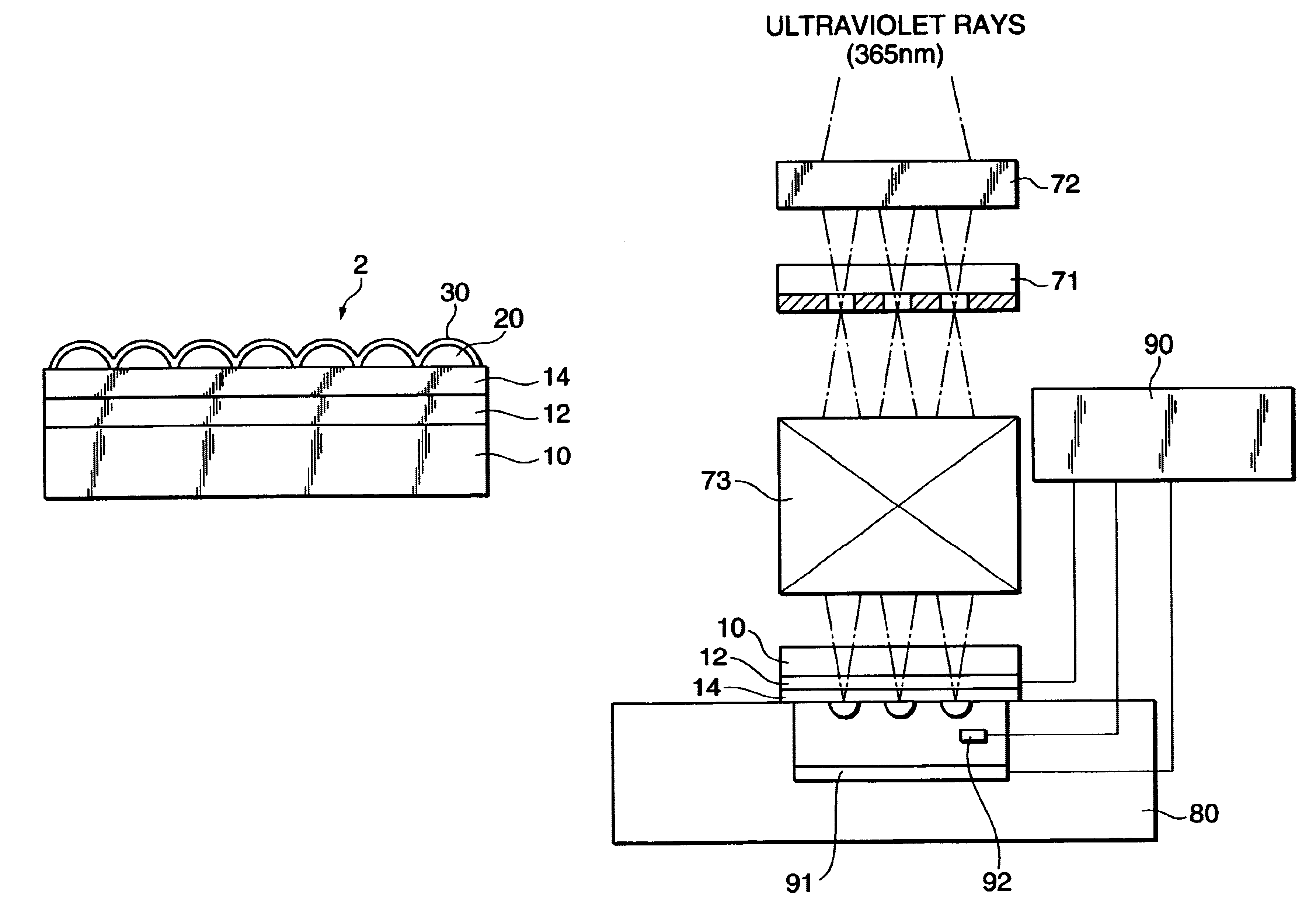
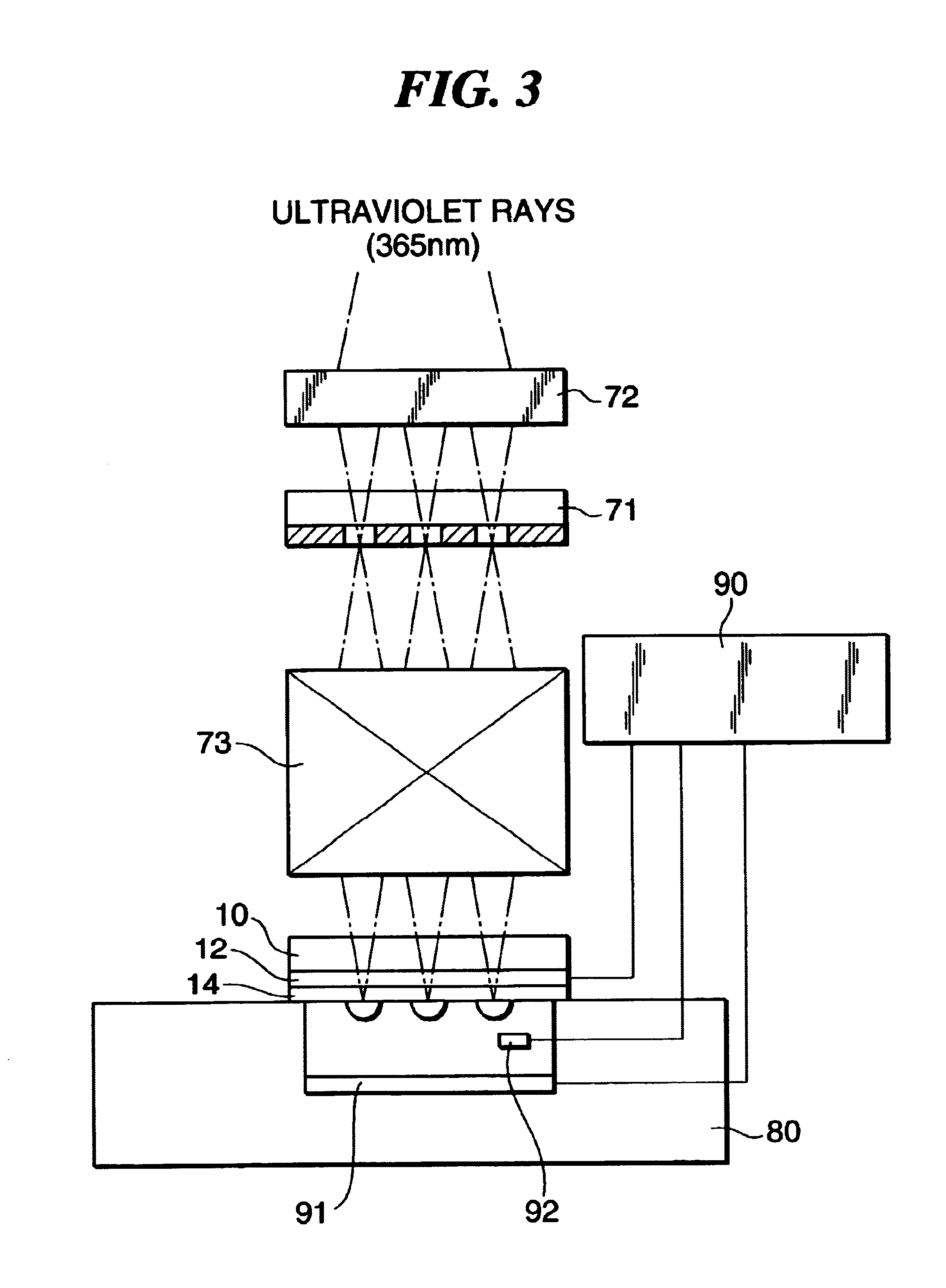
A three-electrode type customary electrodeposition apparatus in electrochemistry shown in FIG. 3 was used and a TiO.sub.2 thin film as a micro-lens array preparing substrate was utilized as ...
example 2
Electrodeposition was conducted by use of the same micro-lens array preparing substrate, photo-mask, electrolyte and electrodeposition conditions as those in Example 1 except for using a micro-lens array manufacturing apparatus shown in FIG. 4. A mercury xenon lamp (manufactured by Yamashita Denso Corporation, light intensity: 50 mW / cm.sup.2, wavelength: 365 nm) was used as the exposure device and the photo-mask was made in intimate contact with the glass substrate of the micro-lens array preparing substrate.
Further, heat treatment was applied at 150.degree. C. in the same manner as in Example 1 and a 96-nm SiO.sub.2 film was formed to obtain a micro-lens array.
The same micro-lens array as in Example 1 was obtained.
example 3
Electrodeposition was conducted by use of the same micro-lens array preparing substrate, photo-mask, electrolyte and electrodeposition conditions as those in Example 1 except for using a laser beam exposure device instead of using the projection type exposure device used in Example 1. A laser beam exposure device using an He--Cd laser, operationally associated with a Galvano scanner and an AO modulator and capable of turning on and off the laser beam at a predetermined position was used. The laser beam was formed as a Gaussian beam in which the intensity of light was increased toward the beam center and decreased toward the periphery. Exposure was conducted while scanning by the exposure apparatus.
Further, heat treatment was applied at 150.degree. C. in the same manner as in Example 1 and a 96-nm SiO.sub.2 film was formed to obtain a micro-lens array.
The same micro-lens array as in Example 1 was obtained.
The method of manufacturing the micro-lens array according to this invention ca...
PUM
| Property | Measurement | Unit |
|---|---|---|
| diameter | aaaaa | aaaaa |
| heat resistance | aaaaa | aaaaa |
| heat resistance | aaaaa | aaaaa |
Abstract
Description
Claims
Application Information


