Transfer film, method for forming metal back layer, and image display

a metal back layer and transfer film technology, applied in the field of transfer film, can solve the problems of deteriorating the optical reflection performance of the metal back layer, difficult to keep the baking resistance characteristic in good condition, and conventional transfer methods that were difficult to put into actual use, etc., to achieve remarkable withstand voltage characteristics, high metal back effects, and efficient advantageous effects

Inactive Publication Date: 2005-01-11
KK TOSHIBA +2
View PDF19 Cites 3 Cited by
  • Summary
  • Abstract
  • Description
  • Claims
  • Application Information

AI Technical Summary

Benefits of technology

The present invention has been completed to remedy the above problems, and it is an object of the invention to provide a transfer film capable of forming a metal back layer having good characteristics by a transfer method, a method for forming the metal back layer having remarkable advantageous effects efficiently by the transfer method, and a display device which has a high metal back effect and a remarkable withstand voltage characteristic and can make display with high luminance and high quality.
efficiently by the transfer method, and a display device which has a high metal back effect and a remarkable withstand voltage characteristic and can make display with high luminance and high quality.
As described in claim 1, the transfer film according to a first aspect of the present invention is a transfer film, comprising a base film, a parting-agent layer, a protective film and a metal film, the parting-agent layer, the protective film and the metal film being stacked on the base film, wherein the protective film is mainly formed of a resin and contains at least one kind of softening agent selected from the group of phosphate, aliphatic monobasic ester, aliphatic dibasic ester, dihydric alcohol ester, oxyacid ester, butyl oleate, dibutyl adipate, paraffin chloride, toluenesulfonethylamide, toluenesulfonmethylamide, an aminobenzene sulfonamide compound, a sulfonamide compound, methyl abietate, dinonyl naphthalene, acetyl tributyl citrate, an aminotoluene sulfonamide compound and N-butyl benzene sulfonamide.
In the transfer film according to the first invention, the softening agent is desirably contained in a range of 1 to 30% in a mass ratio against all materials configuring the protective film as described in claim 2. As described in claim 3, it is desirable that the protective film has a thickness of 0.1 to 30 μm. Besides, as described in claim 4, it may be configured to have an adhesive-agent layer on the metal film. And, the adhesive agent can be mainly composed of at least one kind of resin selected from the group of a vinyl acetate resin, an ethylene-vinyl acetate copolymer, a styrene-acrylic acid resin, an ethylene-vinyl acetate-acrylic acid terpolymer, a vinyl chloride-vinyl acetate copolymer, a polybutene resin and a polyamide resin as described in claim 5.
As described in claim 6, the transfer film of the second invention is a transfer film comprising a base film, a parting-agent layer and a transfer layer, the parting-agent layer and the transfer layer being stacked on the base film,
wherein the transfer layer includes a high resistance layer having a surface resistivity of 102 to 108 Ω / □. And, the transfer film of the second invention can be configured in such a way that the transfer layer includes a high resistance layer having a surface resistivity of 102 to 108 Ω / □ and a light reflection layer which is stacked thereon and has a surface resistivity of less than 102 Ω / □ as described in claim 7.

Problems solved by technology

But, such characteristics were hardly realized at the same time and the transfer method was conventionally hard to put into actual use.
Therefore, the decomposition gas generated at this time causes destruction of the metal film such as a blister, and it is difficult to keep the baking resistance characteristic in good condition.
But, such methods had a disadvantage that a side effect was caused to deteriorate the optical reflection performance of the metal back layer.
But, this method is also hard to form a good metal film.
Besides, in the aforementioned lacquer method for forming a metal back layer a metal film is formed on a base surface having large projections and depressions by vacuum deposition, so that it is hard to form a thin film having high reflectance.
Therefore, it was hard to obtain a phosphor screen having high luminance, and especially there was a problem of unevenness in luminance on the phosphor screen of the display such as the FED which operates in a low energy electron beam region.
Furthermore, the FED has a gap (space) of about one to several mm between the face plate having the phosphor screen and the rear plate having the electron-emitting element, and the gap cannot be increased in view of resolution and characteristics of a spacer.
As a result, a high voltage of about 10 kV is applied to generate a strong electric field in the very small gap between the face plate and the rear plate, resulting in a problem that an electric discharge (dielectrical breakdown) tends to be caused.
And, the occurrence of an electric discharge had a tendency of destroying or degrading the electron-emitting element or the phosphor screen.

Method used


Image

  • Transfer film, method for forming metal back layer, and image display
  • Transfer film, method for forming metal back layer, and image display
  • Transfer film, method for forming metal back layer, and image display

Examples


embodiment 1

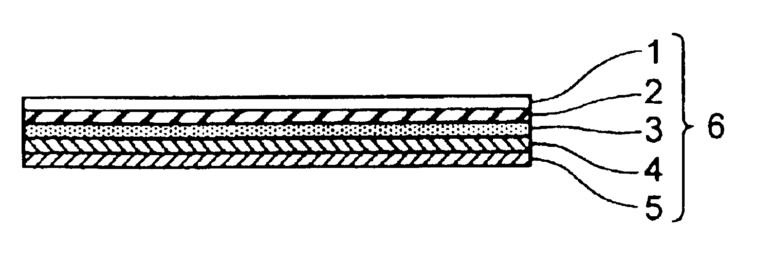
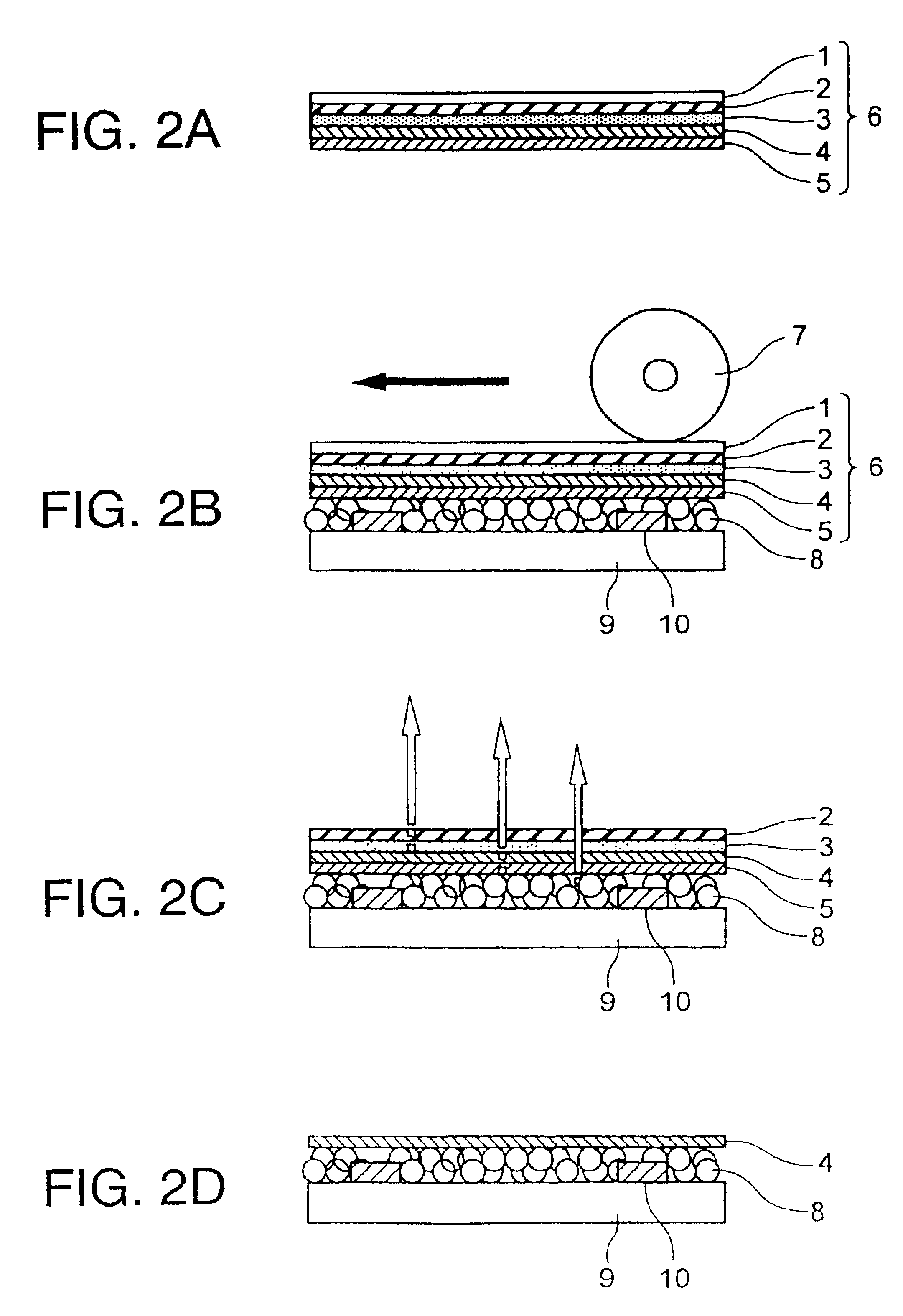
A transfer film was produced by the following procedure. A parting agent consisting of 75 parts of toluene, 12 parts of methyl isobutyl ketone, 12 parts of methyl ethyl ketone, 0.2 part of acetylene glycol, 0.2 part of waxes, 0.2 part of cellulose acetate, 0.2 part of a rosin-based resin and 0.2 part of a silicone resin was applied to a base film made of a polyester resin having a thickness of 20 μm by a gravure coater and dried to form a parting-agent layer having a thickness of 0.5 μm.

Then, a resin composition consisting of 25 parts of methyl isobutyl ketone, 25 parts of methyl ethyl ketone, 6 parts of denatured alcohol, 10 parts of toluene, 10 parts of butyl acetate, 10 parts of ethyl acetate, 5 parts of a melamine resin, 5 parts of a urea resin, 1 part of cellulose derivative, 1 part of a rosin-based resin, 1 part of dimethylsiloxane, 0.5 part of phosphoric acid and 0.5 part of p-toluenesulfonic acid was applied to the parting-agent layer by the gravure coater and dried to form ...

embodiment 2

First, a transfer film was produced according to the following procedure. A parting agent consisting of 75 parts of toluene, 12 parts of methyl isobutyl ketone, 12 parts of methyl ethyl ketone, 0.2 part of acetylene glycol and 0.2 part of a silicone resin was applied to a base film made of a polyester resin having a thickness of 20 μm by a gravure coater and dried to form a parting-agent layer having a thickness of 0.5 μm. Then, a resin composition consisting of 25 parts of methyl isobutyl ketone, 25 parts of methyl ethyl ketone, 6 parts of denatured alcohol, 10 parts of toluene, 10 parts of butyl acetate, 10 parts of ethyl acetate, 5 parts of a melamine resin, 5 parts of a urea resin, 1 part of a cellulose derivative, 1 part of a rosin-based resin, 1 part of dimethylsiloxane, 0.5 part of phosphoric acid, 0.5 part of p-toluenesulfonic acid and 2 parts of N-butyl benzene sulfonamide was applied to the parting-agent layer by the gravure coater and dried to form a protective film havin...

embodiment 3

In the same way as in Embodiment 2, a transfer film was produced except that the aluminum film had a thickness of 50 nm.

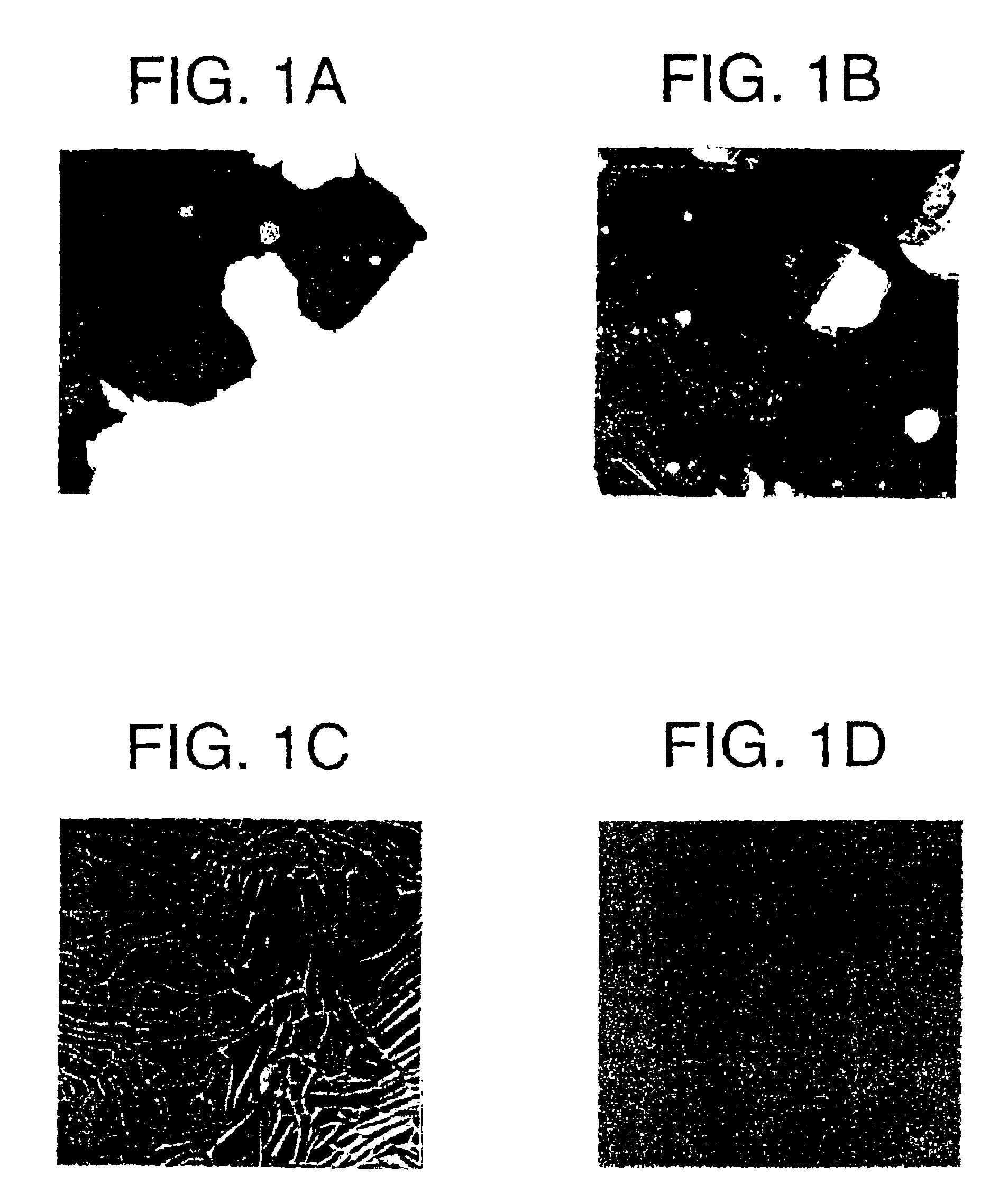
Then, a stripe-pattern light shielding layer made of a black pigment was formed on one side of a face plate for a 10-inch FED by a screen printing method. A phosphor layer having three colors red (R), green (G) and blue (B) was formed between the light shielding section and the light shielding section of the light shielding layer by the screen printing method in such a way that the respective colors were adjacent to one another in the form of a stripe.

Then, a transfer film was disposed so to have its adhesive-agent layer come into contact with the phosphor layer, pressed by a rubber roller having hardness of 50 degrees and a surface temperature of 200° C. at a velocity of 2 m / min. and a pressing force of 300 kg / cm2. And the base film was peeled at a velocity of 10 m / min., to form an aluminum film on the phosphor layer of the face plate. Then, the face plate was rai...


PUM

PropertyMeasurementUnit
thicknessaaaaaaaaaa
resistanceaaaaaaaaaa

Abstract

A transfer film comprising a base film (11), a parting-agent layer (12), a protective film (13), and a metal film (14), the latter three being formed on the base film (11) in order, wherein the protective film (13) contains a softening agent such as a phosphate, an aliphatic monobasic acid ester, an aliphatic dibasic acid ester, or a dihydric alcohol ester. By using such a transfer film, a metal back layer is formed. Since the transfer layer of the transfer film has a surface resistivity of as high as 102-108 Ω / , the surface resistivity of the formed metal back layer is high, and discharge is suppressed.

Description

TECHNICAL FIELDThe present invention relates to a transfer film, a method for forming a metal back layer of a phosphor screen by using the transfer film, and an display device having the metal back layer.BACKGROUND ARTConventionally, for the phosphor screen of a cathode ray tube (CRT), a field emission type display (FED) and the like, a metal back type structure in which a metal film is formed on the inner surface (surface opposite to a face plate) of a phosphor layer is adopted extensively. In the light emitted from a phosphor by the electrons discharged from an electron source, this metal back layer reflects the light, which advances toward the electron source, to the face plate side to improve luminance and to stabilize the potential of the phosphor layer. It also has a function to prevent the phosphor layer from being damaged by ions which are generated when the gas remaining in a vacuum envelop is ionized.The metal back layer is conventionally formed by a method (lacquer method...

Claims


Application Information

Patent Timeline
Patent Type & Authority Patents(United States)
IPC IPC(8): H01J29/28H01J29/18
CPCH01J29/28H01J31/123Y10T428/253Y10T428/265Y10T428/1476H01J2329/28Y10T428/31692Y10T428/31681H01J9/22
Inventor ITO, TAKEOTANAKA, HAJIMENAKAZAWA, TOMOKONAKAYAMA, TAICHIROSHINOHARA, TAKAAKINAKAYAMA, YOICHIROSAKAI, KAZUO
Owner KK TOSHIBA
Why Eureka
Try Eureka