

Transparent conductive layer composition, transparent conductive layer formed of the composition, and image display having the transparent conductive layer
a technology of transparent conductive layer and composition, which is applied in the direction of non-metal conductors, cellulosic plastic layered products, instruments, etc., can solve the problems of inability to form an electromagnetic wave-shielding and anti-reflective conductive layer using a conductive oxide, and the anti-reflective function cannot be expected from the thin conductive layer, so as to improve the anti-reflective and electromagnetic wave-shielding properties and improve the anti-r
- Summary
- Abstract
- Description
- Claims
- Application Information
AI Technical Summary
Benefits of technology
Problems solved by technology
Method used
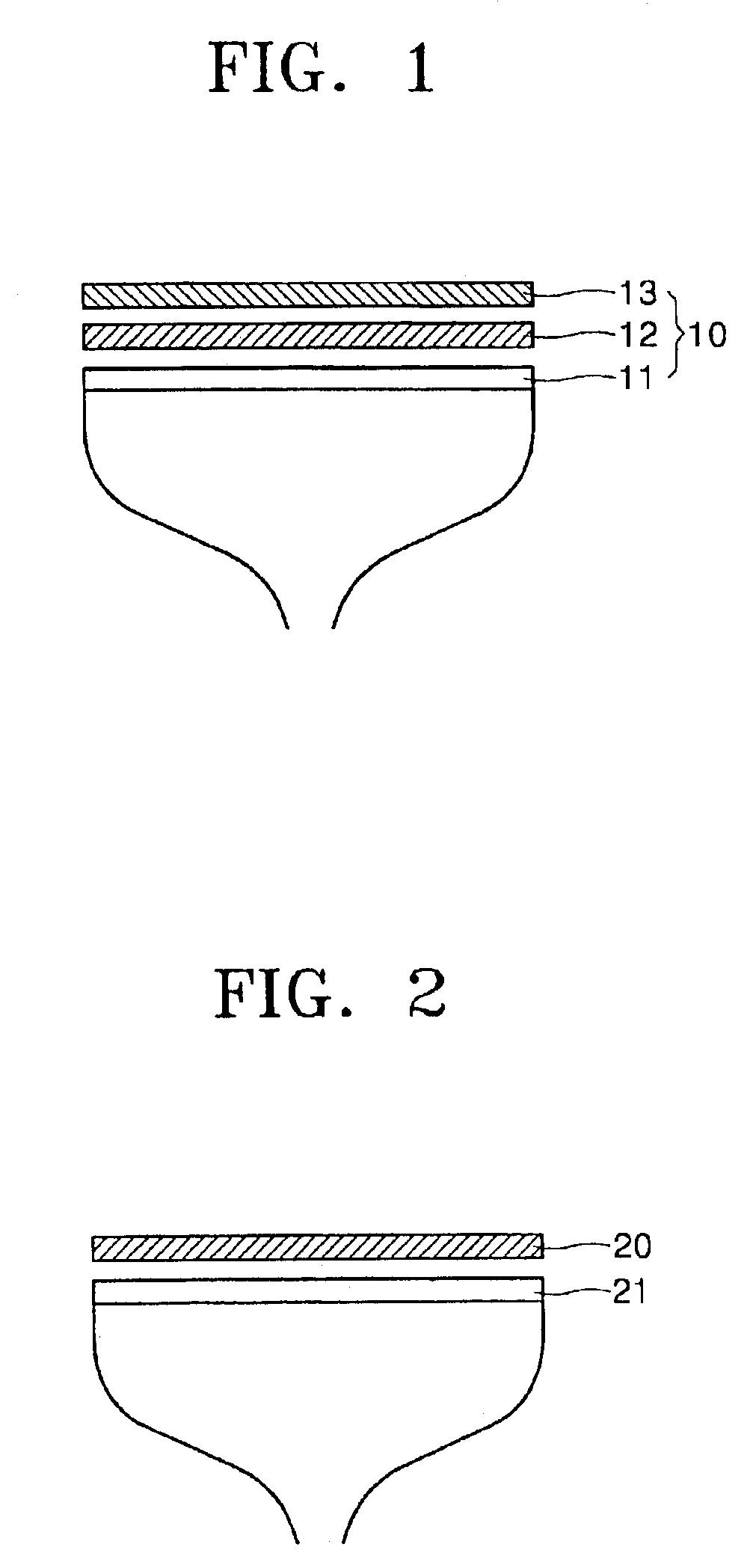
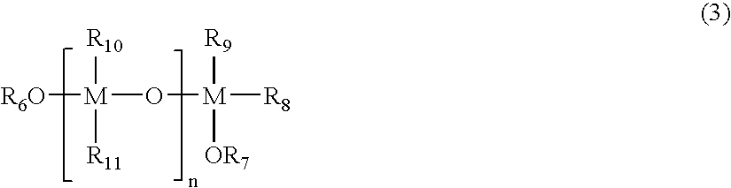
Image

Examples
example 1
A conductive layer composition was prepared by adding 10 g of 5% aqueous suspension of Ag / Pd particles having an average particle diameter of 20 nm into a solvent mixture containing 15 g ethanol, 10 g methanol, 10 g isopropyl alcohol, and 5 g n-butanol.
In addition, a transparent coating layer composition was prepared by mixing 2.67 g tetraethyl orthosilicate and 0.08 g 3-aminopropyltrimethoxysilane with a solvent mixture containing 50 g ethanol, 30 g methanol, 10 g isopropyl alcohol, and 7.25 g n-butanol, and aging the mixture at 60° C. for 24 hours.
A substrate was spin coated with the conductive layer composition, followed by drying at 60° C. to form a conductive layer. Subsequently, the transparent coating layer composition was coated on the conductive layer and subjected to a thermal treatment at 200° C. for 30 minutes to form a transparent coating layer. As a result, a complete transparent conductive layer was obtained.
example 2
A transparent conductive layer was formed in the same manner as in example 1 except that the transparent coating layer composition was changed as follows.
2.67 g tetraethyl orthosilicate and 0.08 g N-(6-aminoethyl)-3-aminopropyltrimethoxysilane was mixed with a solvent mixture containing 50 g ethanol, 30 g methanol, 10 g isopropyl alcohol, and 7.25 g n-butanol, and the mixture was aged at 60° C. for 24 hours to prepare the transparent coating layer composition.
example 3
A transparent conductive layer was formed in the same manner as in example 1 except that the conductive layer composition was changed as follows.
A conductive layer composition was prepared by adding 10 g of 5% aqueous suspension of Ag / Pd particles having an average particle diameter of 20 nm into a solvent mixture containing 30 g ethanol, 5 g methanol, and 5 g isopropylcellosolve.
PUM
| Property | Measurement | Unit |
|---|---|---|
| particle diameter | aaaaa | aaaaa |
| temperature | aaaaa | aaaaa |
| temperature | aaaaa | aaaaa |
Abstract
Description
Claims
Application Information