Electrophoretic display and novel process for its manufacture

a technology of electrophoretic display and manufacturing process, which is applied in the direction of electrographic process apparatus, instruments, optics, etc., can solve the problems of poor scratch resistance, slow response time for a given voltage, and difficulty in partition formation, etc., to achieve low cost production, efficient and inexpensive, and high volume

Inactive Publication Date: 2005-03-08
E INK CALIFORNIA
View PDF120 Cites 67 Cited by
  • Summary
  • Abstract
  • Description
  • Claims
  • Application Information

AI Technical Summary

Benefits of technology

The multiple-step processes as disclosed in the present application may be carried out roll-to-roll continuously or semi-continuously. Consequently, they are suitable for high volume and low cost production. These processes are also efficient and inexpensive as compared to other processes for high volume production operations.
One of the major advantages of the EPDs of the present invention, is that the microcup wall is in fact a built-in spacer to keep the top and bottom substrates apart at a fixed distance. The mechanical properties and structural integrity of microcup displays are significantly better than any prior art displays including those manufactured by using spacer particles. In addition, displays involving microcups have desirable mechanical properties including reliable display performance when the display is bent, rolled or under compression pressure from, for example, a touch screen application. The use of the microcup technology also eliminates the need of an edge seal adhesive which would limit and predefine the size of the display panel and confine the display fluid inside a predefined area. The display fluid within a conventional display prepared by the edge sealing adhesive method will leak out completely if the display is cut in any way, or if a hole is drilled through the display. The damaged display will be no longer functional. In contrast, the display fluid withi...

Problems solved by technology

However, difficulties are encountered in the formation of the partitions, the process of filling the display with a fluid, enclosing the fluid in the display, and keeping the suspensions of different colors separated from each other.
The large microcapsule size results in a poor scratch resistance and a slow response time for a given voltage because a large gap between the two opposite electrodes is required for large capsules.
Also, the hydrophilic shell of microcapsules prepared in an aqueous solution typically resul...

Method used


Image

  • Electrophoretic display and novel process for its manufacture
  • Electrophoretic display and novel process for its manufacture
  • Electrophoretic display and novel process for its manufacture

Examples


example 1

Preparation of Microcups by Microembossing

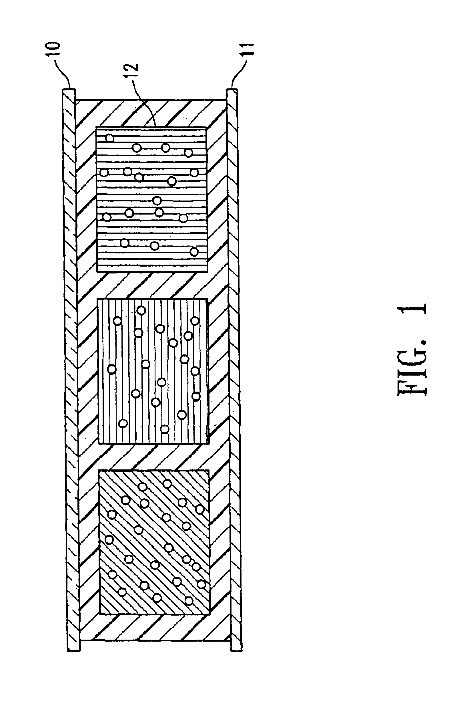
The composition shown in Table 1 is coated onto Mylar J101 / 200 gauge using a Nickel Chrome bird type film applicator with an opening of 3 mil. The solvent is allowed to evaporate leaving behind a tacky film with a Tg below room temperature.

TABLE 1PMMA-containing Composition for MicroembossingNo.DescriptionIngredientSupplierWt %1Epoxy acrylateEbecryl 3605UCB Chemicals7.352MonomerSartomer SR205Sartomer9.593UrethaneEbecryl 6700UCB Chemicals4.87acrylate4Polymethyl-Elvacite 2051ICI9.11methacrylate5PhotoinitiatorDarocur 1173Ciba1.456CationicCyracure UVIUnion Carbide0.60photoinitiator69767SolventAcetoneAldrich67.03Total100.00

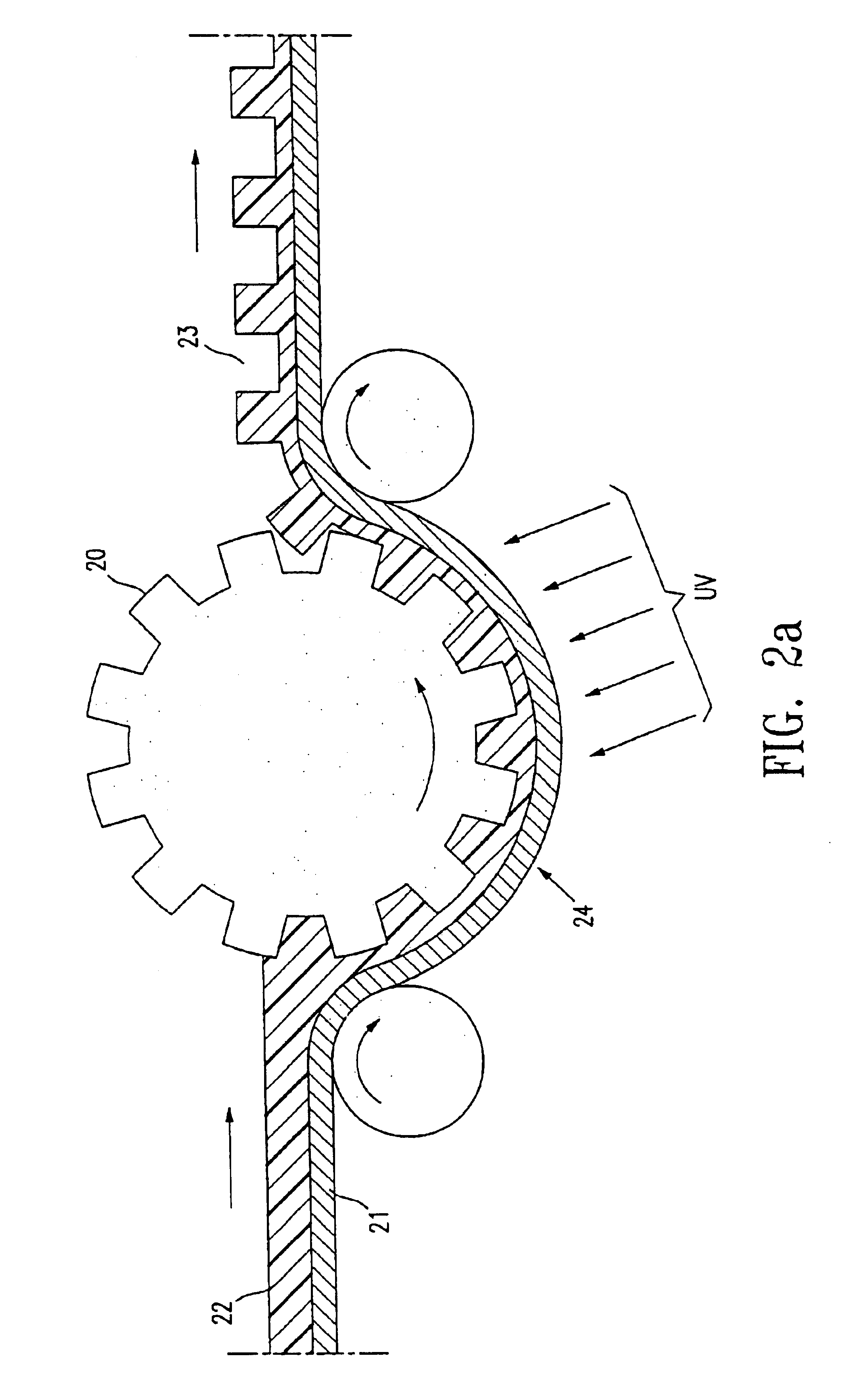
A pre-patterned stencil from Photo Stencil, Colorado Springs, Colo., was used as the male mold for microembossing and Frekote 700-NC from Henkel was used as the mold release. The coated film was then embossed by the stencil using a pressure roller at room temperature. The coating was then UV cured for about 20 minutes through t...

example 2

A composition containing solid oligomer, monomer and additive is shown in Table 2. The glass transition temperature of the mixture is again below room temperature. The tacky coating is deposited on top of Mylar J101 / 200 gauge as before. Embossing can be conducted at 32° C. and 60° C. using a heated pressure roller or laminator. Well-defined high resolution microcups (100-400 dpi) with depth ranging from 5-30 microns were produced.

TABLE 2Embossing CompositionNo.DescriptionIngredientSupplierWt %1Epoxy acrylateEbecryl 3903UCB Chemicals17.212MonomerHDODAUCB Chemicals8.613Urethane acrylateEbecryl 4827UCB Chemicals2.874PhotoinitiatorIrgacure 500Ciba1.435SlipEbecryl 1360UCB Chemicals1.606SolventAcetoneAldrich68.26Total100

example 3

A primer solution comprising of 5 parts of Ebecryl 830, 2.6 parts of SR-399 (from Sartomer), 1.8 parts of Ebecry 1701, 1 part of PMMA (Mw=350,000 from Aldrich), 0.5 parts of Irgacure 500 and 40 parts of methyl ethyl ketone (MEK) was coated onto a 2 mil 60 ohm / sq. ITO / PET film (from Sheldahl Inc., MN.) using a #3 Myrad bar, dried, and UV cured by using the Zeta 7410 (5 w / cm2, from Loctite) exposure unit for 15 minutes in air.

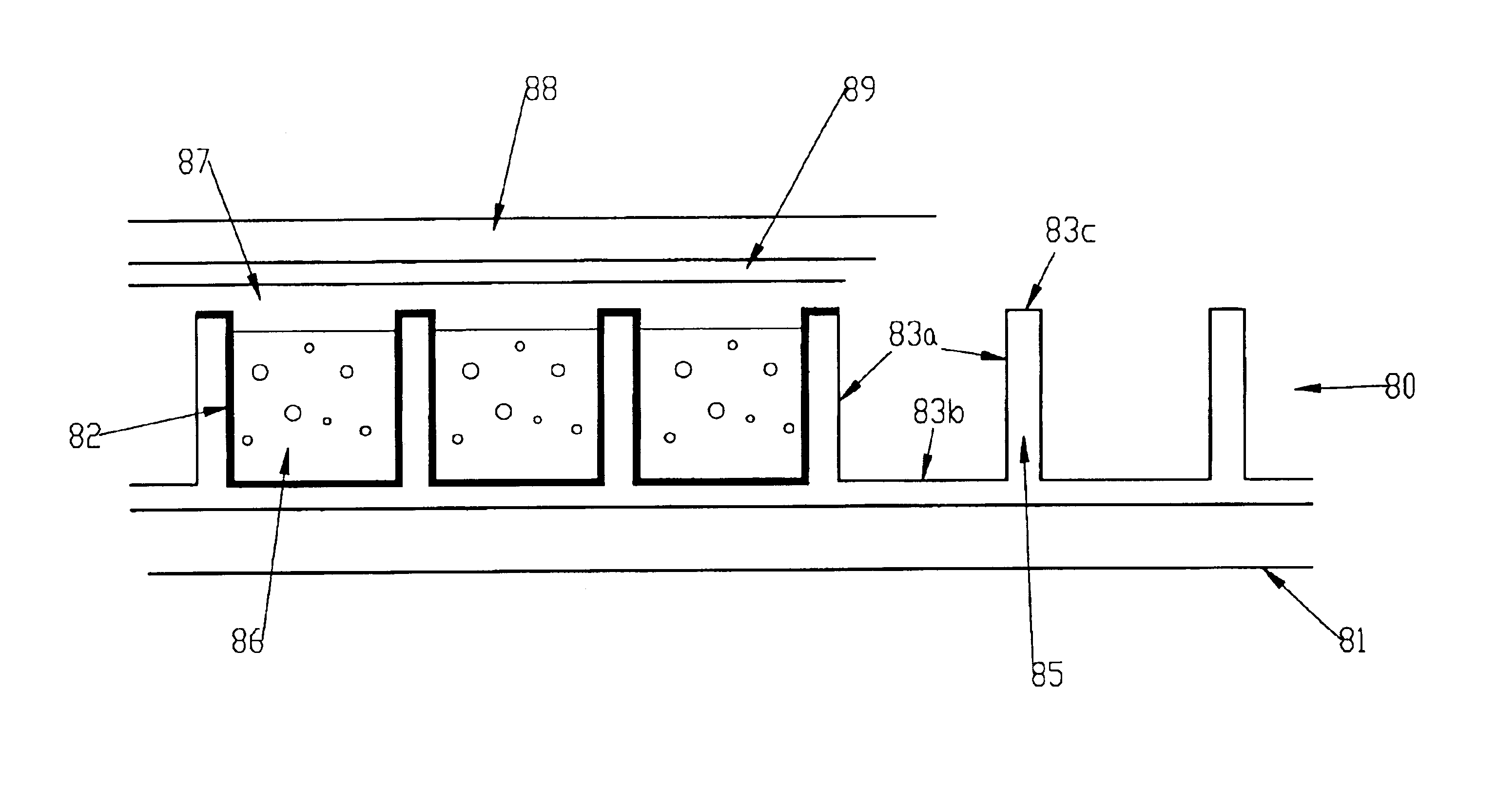
35 Parts by weight of Ebecryl 600 (UCB), 40 parts of SR-399 (Sartomer), 10 parts of Ebecryl 4827 (UCB), 7 parts of Ebecryl 1360 (UCB), 8 parts of HDDA (UCB), 0.05 parts of Irgacure 369 (Ciba Specialty Chemicals) and 0.01 parts of isopropyl thioxanthone (ITX from Aldrich) were mixed homogeneously, coated onto the primer treated ITO / PET film with a targeted thickness of about 50 μm, and embossed with a Ni—Co male mold having a 60 (length)×60 (width) μm repetitive protrusion square pattern with 25-50 μm protrusion height and 10 μm wide partition lines, UV cured from...


PUM


Abstract

This invention relates to an electrophoretic display comprising cells of well-defined shape, size and aspect ratio which cells are filled with charged pigment particles dispersed in a solvent, and novel processes for its manufacture.

Description

BACKGROUND OF THE INVENTIONa) Field of the InventionThe application claims an invention directed to an electrophoretic display comprising isolated cells of well-defined shape, size and aspect ratio which cells are filled with charged pigment particles dispersed in a dielectric solvent and sealed, and novel processes for its manufacture.b) Description of Related ArtThe electrophoretic display (EPD) is a non-emissive device based on the electrophoresis phenomenon of charged pigment particles suspended in a solvent. It was first proposed in 1969. The display usually comprises two plates with electrodes placed opposing each other, separated by using spacers. One of the electrodes, typically on the viewing side, is transparent. For the passive type of EPDs, row and column electrodes on the top (the viewing side) and bottom plates respectively are needed to drive the displays. In contrast, an array of thin film transistors (TFT) on the bottom plate and a common, non-patterned transparent ...

Claims


Application Information

Patent Timeline
IPC IPC(8): G02F1/01G02F1/167
CPCG02F1/167G02F1/133305G02F1/133377G02F2001/1672G02F1/1339G02F1/1681
Inventor LIANG, RONG-CHANGTSENG, SCOTT C-JWU, ZARNG-ARH GEORGEZANG, HONG MEI
Owner E INK CALIFORNIA
Why Eureka
Try Eureka