Photolithography method including a double exposure/double bake

a photolithography and double exposure technology, applied in the field of photolithography process, can solve the problems of limited feature width of patterned area, half-tone masks, and about twice as expensive as binary masks, and achieve the effect of wide process window and small variability

Inactive Publication Date: 2005-04-19
PROMOS TECH INC
View PDF7 Cites 20 Cited by
  • Summary
  • Abstract
  • Description
  • Claims
  • Application Information

AI Technical Summary

Benefits of technology

[0007]The embodiments may also include the use of two photoresist baking steps in addition to the two exposure steps in the photoresist processing. The first baking step takes place after the first exposure, and the second baking step takes place after the second exposure. The two baking steps evaporate moisture from the film, causing the film to shrink slightly, and activate a photo acid generator (PAG) in the photoresist film. The thinner remaining film may require less incident light intensity in the second exposure to convert the photoresist, and the aperture in the photoresist may be widened slightly by the activation of the PAG. Because the photoresist film is thinner, it attenuates a smaller proportion of the incident light beam throughout its depth. Therefore, the variability of the incident energy, as a function of depth in the photoresist film, is narrower. As thinner films may have a smaller variability than thicker films, they may result in a wider process window. A wider process window is important in designing a capable process, which generates repeatable results in the face of some variability in input parameters.
[0008]The embodiments may include use of a binary bias mask during one or both of the exposure steps, whose features have a wider diameter than the eventual feature size on the surface of the photoresist. The bias mask allows an area to be illuminated which is larger than the eventual feature size. Therefore, the bias mask may allow some misregistration of the wafer in the second exposure, compared to its position in the first exposure, as a process tolerance for the double exposure procedure.

Problems solved by technology

In general, the minimum feature width of the patterned area is limited by the wavelength of the particular light source used, due to diffraction effects.
Half-tone masks, however, are about twice as expensive as binary masks.

Method used


Image

  • Photolithography method including a double exposure/double bake
  • Photolithography method including a double exposure/double bake
  • Photolithography method including a double exposure/double bake

Examples


experiment 1

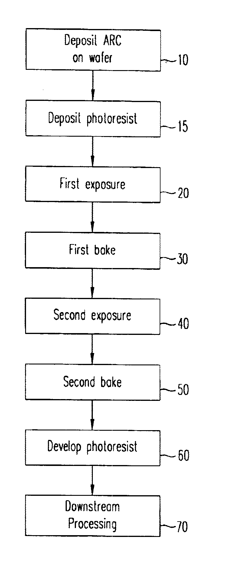
[0039]A first wafer, test wafer #1, was processed according to the flow chart shown in FIG. 2. The wafer is formed of silicon and provided with a layer of polysilicon to a depth of about 80 nm. A layer of an anti-reflection coating and deep UV photoresist are then provided, as set forth in the above discussion. Because polysilicon has a relatively rough surface topography, the edge definition of features created on the polysilicon surface can be expected to be somewhat less well defined than features created on a smooth surface of, for example, bare silicon. A second test wafer, test wafer #2 is a bare silicon wafer having the same anti-reflection coating and deep UV resist layer. However, the second wafer is exposed with a single exposure and processed using a single bake following the exposure to provide a comparison with the double exposure / double bake method applied to test wafer #1. The test array pattern on test wafer #2 was created using an exposure energy of 32 mj / cm2, with ...

experiment 2

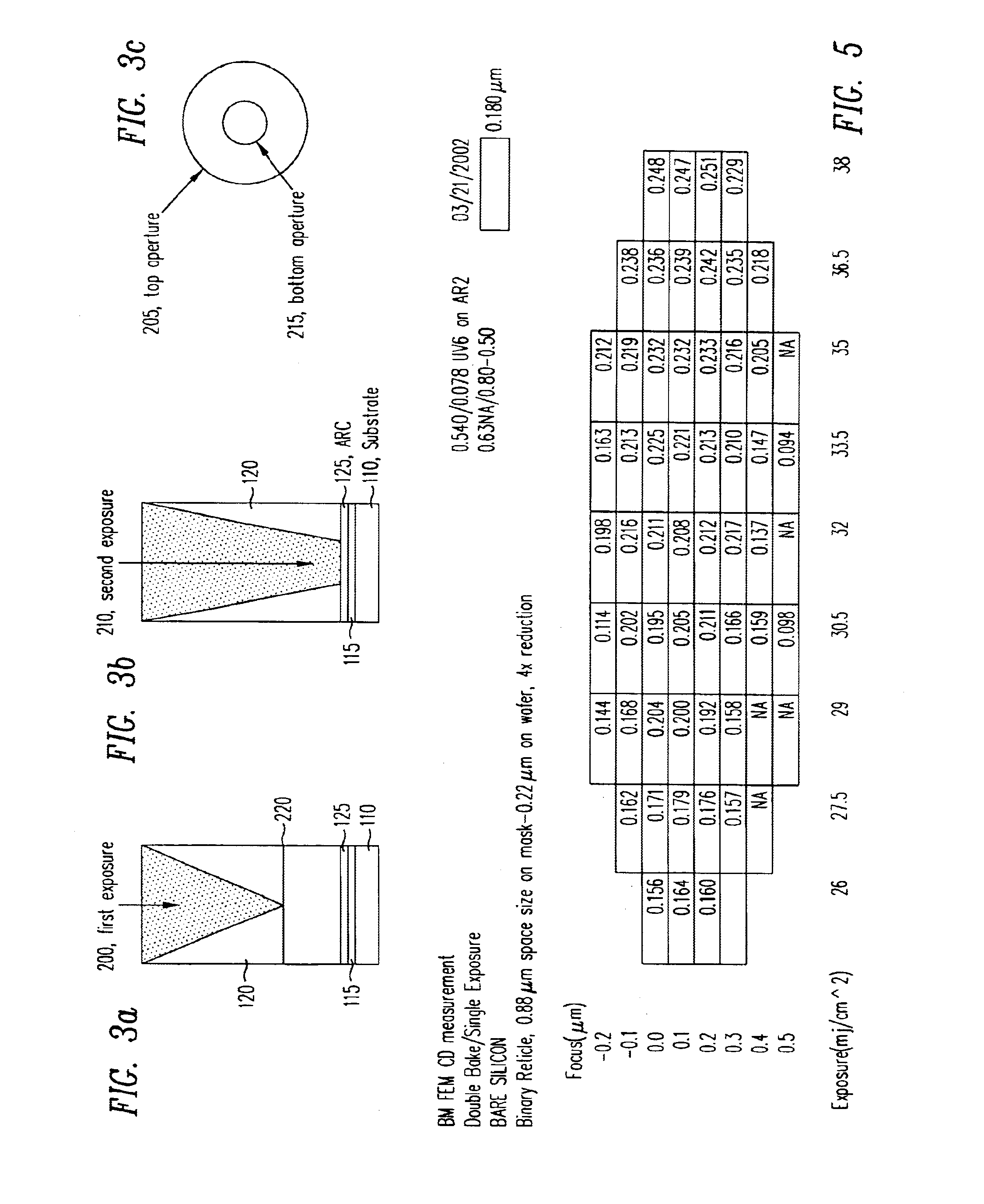
[0042]A third wafer, test wafer #3, is a bare silicon wafer with an anti-reflection coating and deep UV resist layers, as discussed above. Test wafer #3 is processed using a single exposure, but with a double bake, to compare the effects of the different exposure processes with the same baking procedure. The results are similar to those found for the single exposure, single baked wafer, test wafer #2, shown in FIG. 4b. The results for this test wafer #3 are given in FIG. 5. As can be seen from the data, a 0.4 μm focus process latitude is shown for the 0.18 μm contacts, but there is little process latitude in exposure energy, and little focus latitude for the other target contact dimensions. Therefore, a photoresist process with a second exposure followed by a second baking step results in a wider process latitude, than photoresist process with a single exposure followed by a double bake step.

experiment 3

[0043]Finally, two more silicon wafers, test wafers #4 and #5, each coated with an 80 nm layer of polysilicon, an anti-reflection coating and a deep UV photoresist layer, were processed according to the method of FIG. 2, and printed with the test array of points as described above in relation to FIG. 4a. The center of the process window for the second exposure was 18.5 mj / cm2, and 0.1 μm focus for these data, and the target contact hole size was 0.18 μm. The exposure was varied by 0.5 mj / cm2 per column and 0.1 μm focus per row. The data are shown in FIG. 6, and are presented to show process repeatability and to confirm the findings shown in FIG. 4a. As can be seen from the data, the process yields repeatable results between the two wafers #4 and #5, to within about 3% at the center of the process windows for the target values, and to within about 10% at the edges of the process windows. The process latitude on depth of focus is about 0.5 μm, and the exposure latitude is again about ...


PUM


Abstract

A photoresist exposure process is disclosed which produces features which are substantially smaller than the aperture dimension of the mask used to make the feature. The smaller feature size results from a double exposure of the photoresist, combined with a double baking process to create the features in the photoresist. The double baking process thins the layer of photoresist, prior to the second exposure, thereby improving the resolution of the mark created by the second exposure on the photoresist. The process also uses a binary bias mask through which the first exposure is made, which overlaps with the area of the second exposure, to allow a process tolerance for the realignment of the mask over the wafer for the second exposure.

Description

FIELD OF THE INVENTION[0001]The present invention includes a photolithographic process for printing integrated circuit structures on the surface of a substrate.BACKGROUND OF THE INVENTION[0002]Photolithography is widely used to form patterns on semiconductor wafers during fabrication of integrated circuits. A semiconductor wafer 110 (FIG. 1) including an optional topmost layer 115 is coated with a photoresist layer 120. Photoresist 120 is irradiated from a light source 130 through an annular aperture 160. A mask or reticle 140 is placed between source 130 and photoresist 120. Binary mask 140 carries a pattern consisting of opaque and clear features. This pattern defines which areas of photoresist 120 are exposed to the light from source 130. After the exposure, the photoresist 120 is developed so that some of the photoresist is removed to uncover the underlying surface of layer 115 on substrate 110. If the photoresist is “positive,” then the photoresist is removed where it was expos...

Claims


Application Information

Patent Timeline
Patent Type & Authority Patents(United States)
IPC IPC(8): G03F7/20
CPCG03F7/70466
Inventor CAUCHI, JOHNLOU, ERIC
Owner PROMOS TECH INC
Why Eureka
Try Eureka