Layer transfer of low defect SiGe using an etch-back process

Inactive Publication Date: 2005-05-10
GLOBALFOUNDRIES INC
View PDF21 Cites 54 Cited by
  • Summary
  • Abstract
  • Description
  • Claims
  • Application Information

AI Technical Summary

Benefits of technology

[0006]The invention provides a method capable of transferring a low defect SiGe layer onto a desirable substrate using the etch-back method but without any additional heavily doped etch-stop layer. The key feature of this invention is that a SiGe layer serves both as the layer over which the epitaxial strained Si/SiGe is grown but also as

Problems solved by technology

However, the underlying conducting substrate for MODFETs and HBTs or the interaction of the underlying substrate with active design region in CMOS are undesirable features which limit the full implementation of high speed devices.
However, this method has several limits because the oxygen implantation induces further damages in the relaxed SiGe layer in addition to the existing defects caused by l

Method used


Image

  • Layer transfer of low defect SiGe using an etch-back process
  • Layer transfer of low defect SiGe using an etch-back process
  • Layer transfer of low defect SiGe using an etch-back process

Examples


Embodiment Construction

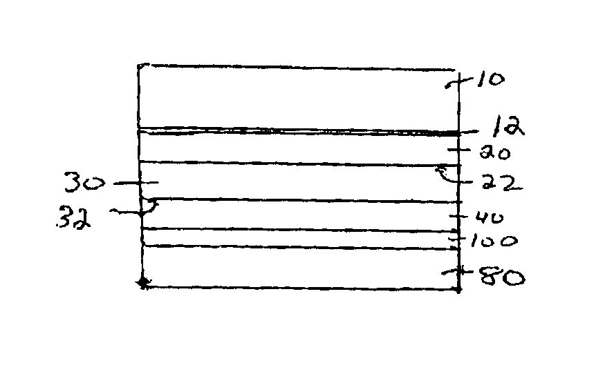
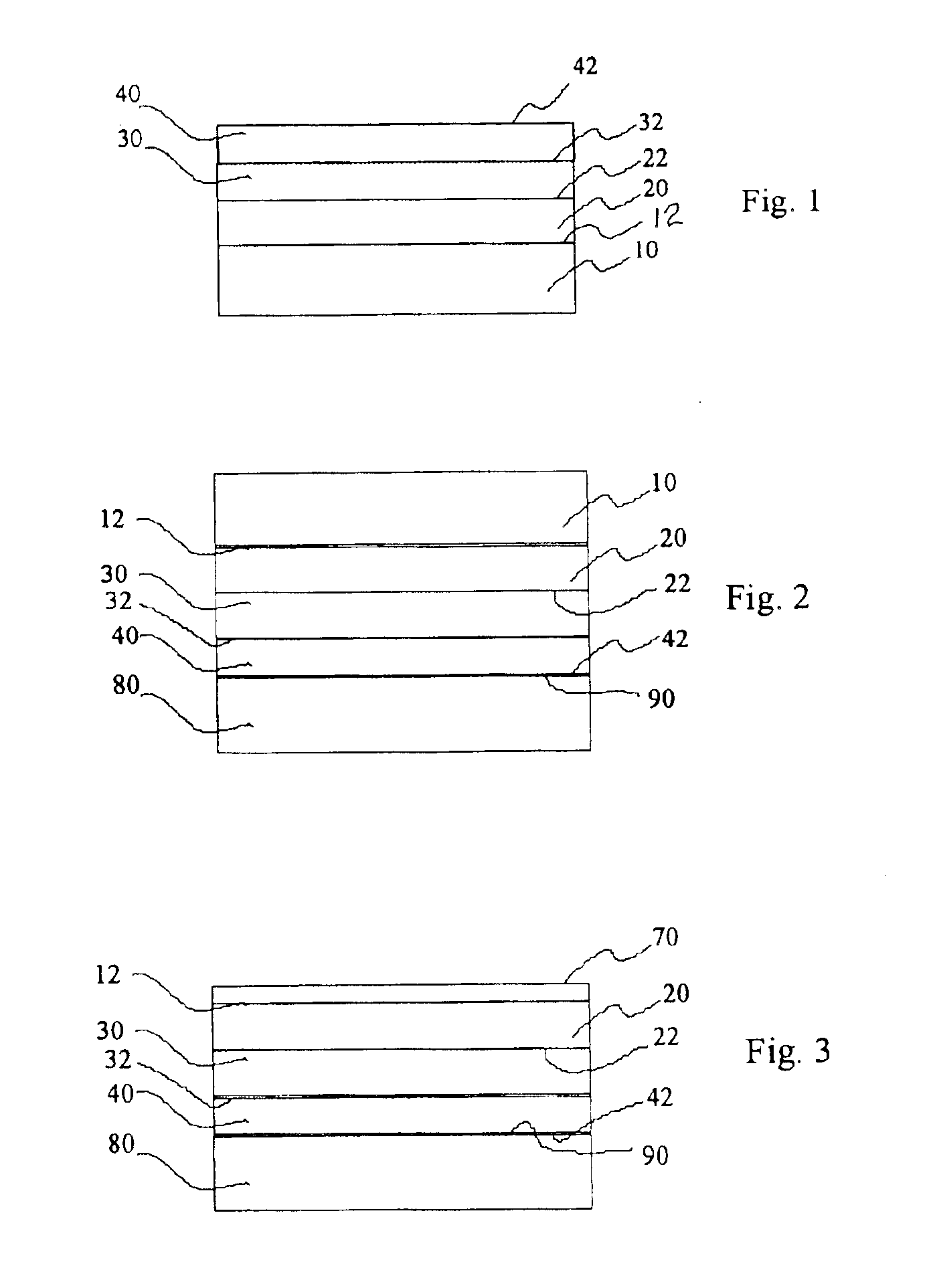
[0017]The embodiment which will now be described in conjunction with the above drawings relates to the formation of a layer of monocrystalline strained Si / SiGe on an insulator material (SGOI) or a SiGe layer on Si with the aid of planarization of surfaces, wafer bonding and a selective wet etching process using SiGe as the etch-stop layer.

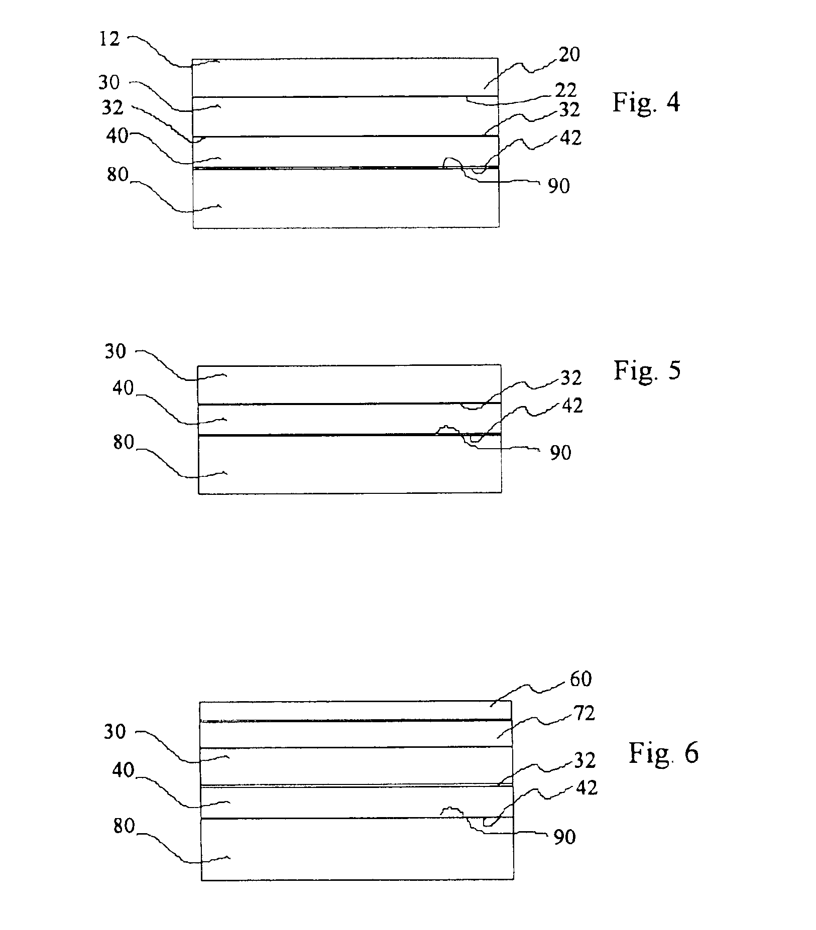
[0018]The top surface of layer 40 shown in FIG. 1 is turned upside down and bought into intimate contact with surface 90 of substrate 80. The two surfaces 42 and 90 are brought together by the wafer bonding approach. The bonded surfaces of 42 and 90 are annealed at a temperature in the range from about 20° C. to about 500° C. for a time period in the range from about 2 hours to about 50 hours. Another embodiment, as shown in FIG. 7, uses at least one intermediate agent layer 100 such as Ge, or metal materials which either have a low-melting point or react with silicon to form a silicide such materials may be tungsten (W), cobalt (Co), titanium (Ti)...


PUM


Abstract

A method for forming strained Si or SiGe on relaxed SiGe on insulator (SGOI) or a SiGe on Si heterostructure is described incorporating growing epitaxial Si1-yGey layers on a semiconductor substrate, smoothing surfaces by Chemo-Mechanical Polishing, bonding two substrates together via thermal treatments and transferring the SiGe layer from one substrate to the other via highly seletive etching using SiGe itself as the etch-stop. The transferred SiGe layer may have its upper surface smoothed by CMP for epitaxial deposition of relaxed Si1-yGey, and strained Si1-yGey depending upon composition, strained Si, strained SiC, strained Ge, strained GeC, and strained Si1-yGeyC or a heavily doped layer to make electrical contacts of the SiGe/Si heterojunction diodes.

Description

FIELD OF INVENTION[0001]This invention relates to transferring a SiGe layer onto a second substrate and forming a new material structure that has emerging applications in microelectronics and optoelectronics. In particular, a strained Si / SiGe layer on an insulator structure is useful for fabricating high speed devices such as complementary metal oxide semiconductor (CMOS) transistors, modulation doped field effect transistors (MODFETs), high electron mobility transistors (HEMTs), and bipolar transistors (BTs); SiGe layer on Si heterostructures can be used to produce photodetectors to provide Si-based far infrared detection for communication, surveillance and medical applications.BACKGROUND OF THE INVENTION[0002]For applications in microelectronics, high carrier mobilities are desirable. It has been found that electron mobility in strained Si / SiGe channels is significantly higher than that in bulk Si. For example, measured values of electron mobility in strained Si at room temperatur...

Claims


Application Information

Patent Timeline
IPC IPC(8): H01L21/762H01L21/02H01L21/20H01L21/70H01L21/336H01L21/338H01L27/12H01L29/161H01L21/331H01L29/737H01L29/778H01L29/786H01L29/812H01L29/861H01L31/10
CPCH01L21/76256H01L21/2007H01L21/20
Inventor CHU, JACK OONDIMILIA, DAVID R.HUANG, LIJUAN
Owner GLOBALFOUNDRIES INC
Why Eureka
Try Eureka