Apparatus and method for multi-target physical-vapor deposition of a multi-layer material structure

a multi-layer material and physical vapor deposition technology, applied in vacuum evaporation coatings, electrolysis components, coatings, etc., can solve the problems of periodic laminated multi-layer structures that have similar difficulties, require more processing steps for material stacks for gmr read sensors, and require more processing steps, so as to achieve effective in-situ cleaning of substrates and/or pvd targets, improve the uniformity of each deposition layer, and improve the effect of film thickness

Inactive Publication Date: 2005-06-14
CVC PRODS
View PDF18 Cites 102 Cited by
  • Summary
  • Abstract
  • Description
  • Claims
  • Application Information

AI Technical Summary

Benefits of technology

[0020]Another technical advantage of the present invention is precise control over film thickness for any of the films in a multi-layer stack which allows deposition of thin layers to fabricate various high-performance device structures including spin-valve GMR, tunneling MRAM, and semiconductor interconnect material systems. The shutter mechanism can provide precise control of stabilized deposition time for each PVD target resulting in improved uniformity for each deposition layer. Moreover, it allows effective in-situ cleaning of the substrate and/or the PVD targets.
[0021]Another import...

Problems solved by technology

Thus, creating material stacks for GMR read sensors generally required more processing steps, including more complicated equipment and fabrication techniques for high-yield manufacturing of high-performance GMR thin-film heads.
Similar difficulties can occur with periodic laminated multi-layer structures, such as laminated flux guide structures of iron, tantalum and silicon di-oxide.
The precision-controlled deposition of materials onto a substrate to create the multi-layer structures that can use the GMR effect is a difficult and time consuming process which requires high-performance vacuum deposition equipment, including plasma sputtering, ion-beam and evaporation processes.
Although conventional physical-vapor deposition (PVD) technology can create GMR-capable structures, each layer of a structure must be carefully deposited in sequence in a time-consuming seque...

Method used


Image

  • Apparatus and method for multi-target physical-vapor deposition of a multi-layer material structure
  • Apparatus and method for multi-target physical-vapor deposition of a multi-layer material structure
  • Apparatus and method for multi-target physical-vapor deposition of a multi-layer material structure

Examples


Embodiment Construction

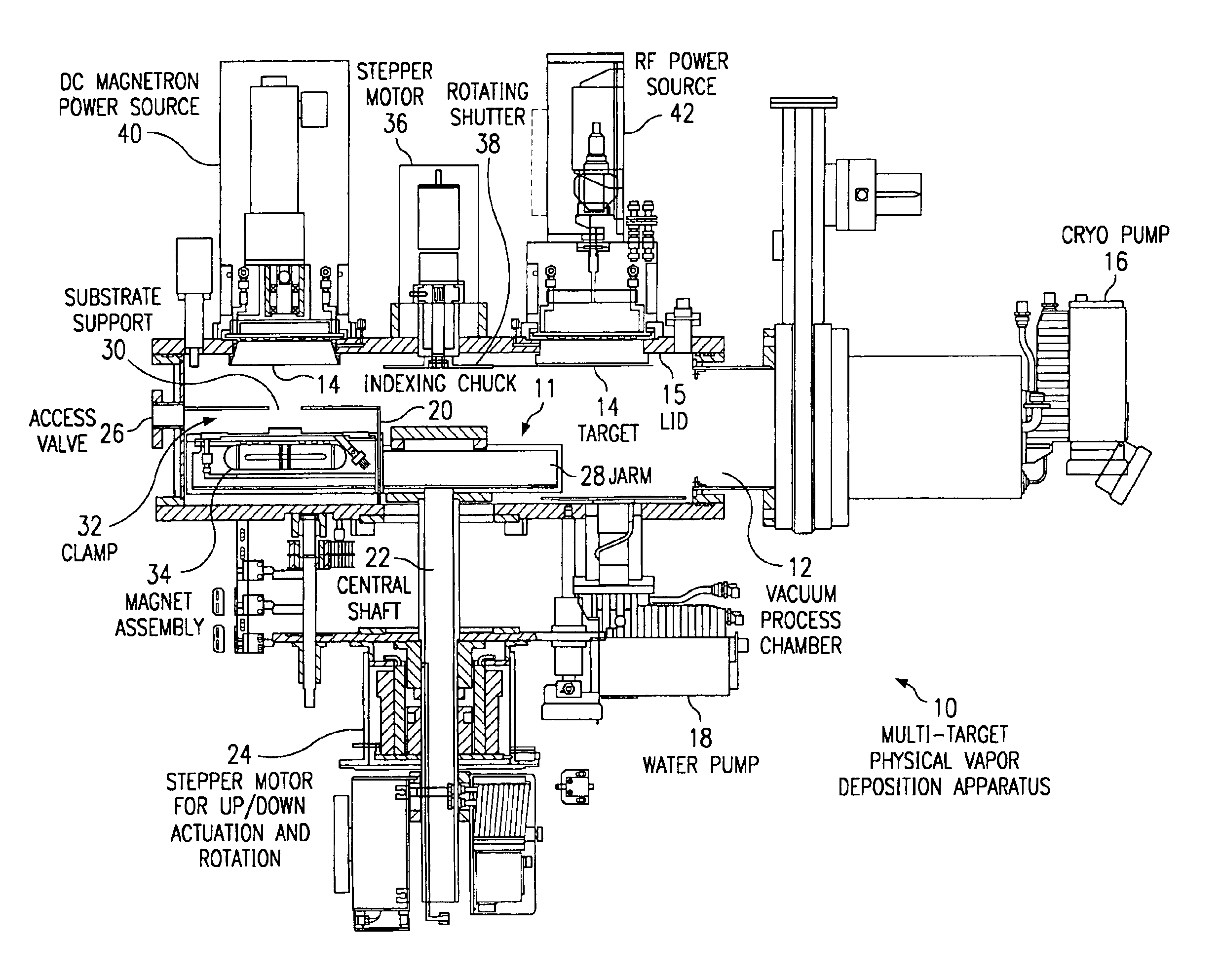
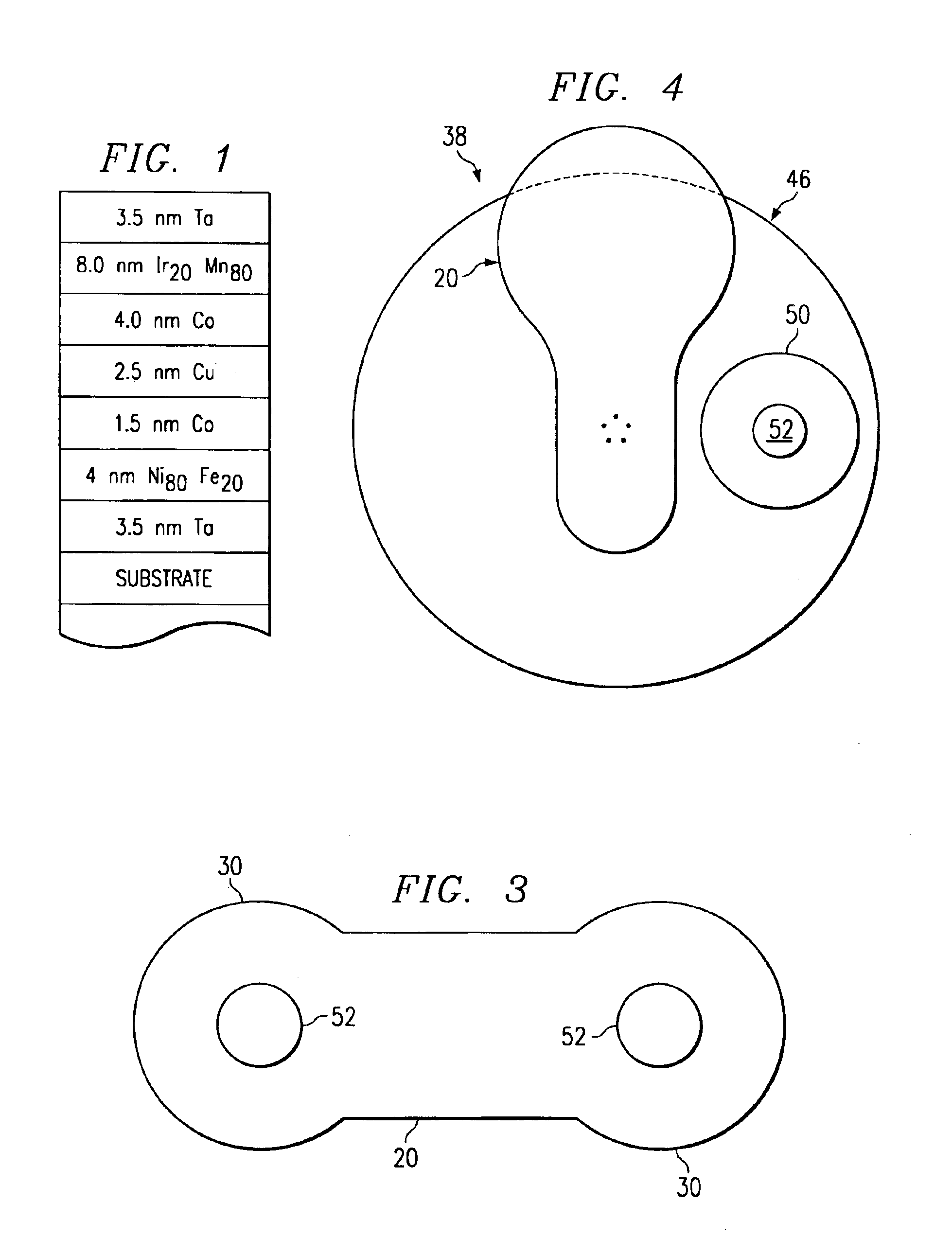
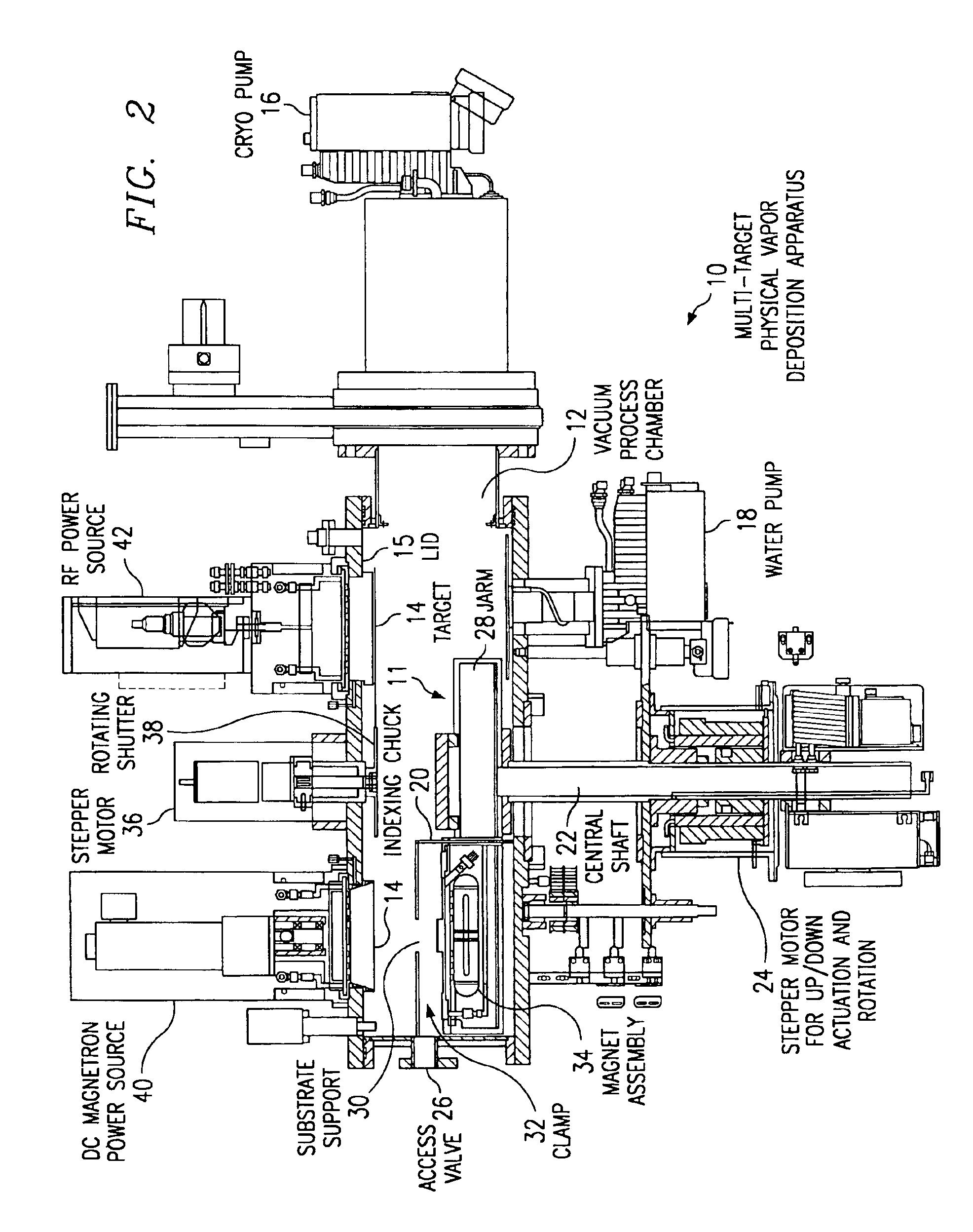
[0031]Preferred embodiments of the present invention are illustrated in the figures, like numerals being used to refer to like and corresponding parts of the various drawings.

[0032]Physical-vapor deposition or PVD is a well-known technique for depositing thin layers of materials onto a substrate for a variety of semiconductor, data storage, optoelectronics, and other applications. Plasma sputtering or plasma PVD is the most widely accepted PVD technique for deposition of various material layers. A power source, such as a DC magnetron or RF magnetron or an RF diode power source, creates power differential between a target assembly comprising the cathode and an anode ring in order to produce a plasma medium between the target and the substrate within a controlled vacuum environment. This electrical power creates a gas discharge plasma and produces ion bombardment on the target surface (e.g., via argon ions), resulting in sputtering of the target material and sputter deposition of the ...


PUM

PropertyMeasurementUnit
Thicknessaaaaaaaaaa
Pressureaaaaaaaaaa
Poweraaaaaaaaaa

Abstract

An apparatus and method for depositing plural layers of materials on a substrate within a single vacuum chamber allows high-throughput deposition of structures such as these for GMR and MRAM application. An indexing mechanism aligns a substrate with each of plural targets according to the sequence of the layers in the structure. Each target deposits material using a static physical-vapor deposition technique. A shutter can be interposed between a target and a substrate to block the deposition process for improved deposition control. The shutter can also preclean a target or the substrate and can also be used for mechanical chopping of the deposition process. In alternative embodiments, plural substrates may be aligned sequentially with plural targets to allow simultaneous deposition of plural structures within the single vacuum chamber. A monitoring and control device can be wed to optimize equipment state, process state, and wafer state parameters by sensing each respective state during or after the deposition process.

Description

TECHNICAL FIELD OF THE INVENTION[0001]This invention relates in general to the field of fabrication of semiconductor integrated circuits and data storage devices, and more particularly to an improved multi-target physical-vapor deposition apparatus and method of use for controlled deposition of a multi-layer material structure onto a substrate in an ultra clean vacuum processing environment.BACKGROUND OF THE INVENTION[0002]Several important applications, including spin-valve giant magneto-resistive (GMR) thin-film heads and semiconductor integrated circuits, use multi-layer material stacks to perform various electronic signal processing and data storage functions. For instance, semiconductor integrated circuit (IC) applications often include multi-layer interconnect structures comprised of multiple layers of glue / diffusion barrier, interconnect metal, and anti-reflection coating (ARC) films. For instance, some multi-level interconnect structures in semiconductor ICs employ a multi-l...

Claims


Application Information

Patent Timeline
IPC IPC(8): C23C14/56
CPCC23C14/568
Inventor MOSLEHI, MEHRDAD M.DAVIS, CECIL J.MANN, CHRISTOPHER J.JAKUBIK, DWAIN R.PARANJPE, AJIT P.
Owner CVC PRODS
Why Eureka
Try Eureka