Method of fabricating flexible circuits for integrated circuit interconnections

a flexible circuit and integrated circuit technology, applied in the field of flexible circuits, can solve the problems of inconvenient manufacturing of flexible circuits, inability to consistently conduct through holes, repetitive process and time-consuming, etc., and achieve the effects of high yield, low cost and increased conductor thickness

Inactive Publication Date: 2005-07-12
TEXAS INSTR INC
View PDF18 Cites 35 Cited by
  • Summary
  • Abstract
  • Description
  • Claims
  • Application Information

AI Technical Summary

Benefits of technology

[0013]To complete the fabrication of the intermediate base structure for a flex film, additional copper is electroplated onto the surfaces to both increase the conductor thickness, and to seal the connection between the solid Cu via and the copper film on the first surface, thereby insuring robust electrical contact. Subsequently, the copper on both surfaces is photopatterned and etched to provide interconnections and bump solder pads. The patterns on either side are aligned to the vias, thereby eliminating the problems associated with aligning patterns on opposite sides of a film.
[0014]It is further an object of the invention to provide a method for fabricating a flex circuit substrate which has high yield, low cost, and is amenable to mass production. In addition to the etched metal matrix, a die set precisely matched to the etched studs facilitates punching apertures for vias in the film. Reel to reel processing and transport are the preferred techniques for fabrication of substrates which may then be assembled into packages using the same format. However, the processes are not limited to this technique, nor is the specific flex circuit application.
[0015]In an alternate embodiment, a metal embossing tool is coated in the selective raised areas with a thin film of copper which under temperature and pressure adheres to the dielectric film simultaneously with the embossing process. The embossing tool is removed, leaving depressed interconnect patterns, contact pads and / or vias coated with copper. The exposed copper is subsequently plated with copper. The process eliminates patterning and etching in the manufacture of a flex circuit, as well as the need for a solder mask on solder contact surface.

Problems solved by technology

In the case of laser ablation where one via is formed at a time, the process is repetitive and time consuming.
Further, the existing techniques for making conductive vias suffer from difficulties in making the through holes consistently conductive, and in aligning the top and bottom circuits with the vias.
Via conductivity failures occur either as electrical opens or as intermittent contacts resulting from separations in the thin conductor walls during thermal excursions due to expansion mismatch between the conductor and the substrate, from incompletely coating by vapor deposition, from air pockets entrapped in the vias during plating from both sides of the circuit, from fatigue failures of the thin conductors, from marginal conductivity of the filling material, and / or from marginal contact due to misalignment of the circuit and vias.

Method used


Image

  • Method of fabricating flexible circuits for integrated circuit interconnections
  • Method of fabricating flexible circuits for integrated circuit interconnections
  • Method of fabricating flexible circuits for integrated circuit interconnections

Examples


Embodiment Construction

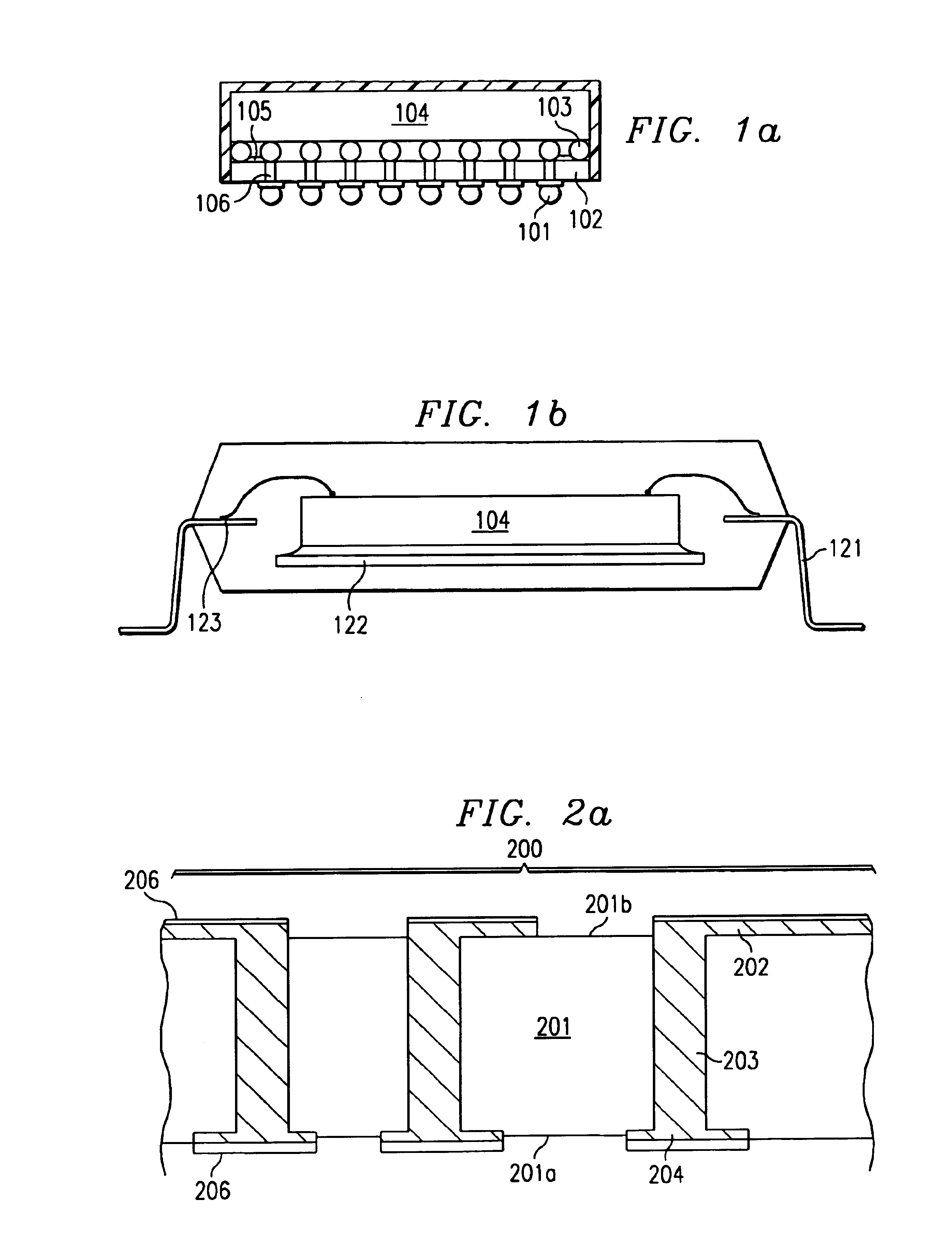
[0027]In accordance with the preferred embodiment of the current invention, a double sided flexible interconnection circuit 200 for use as an integrated package substrate is shown in cross-sectional view in FIG. 2a. The flex circuit includes a base dielectric film 201 of a flexible polymer patterned on the first surface 201a with interconnection traces 202 from the chip terminal pads to conductive vias 203, which provide electrical contact to solder bump contact pads 204 on the second surface 201b of the dielectric film.

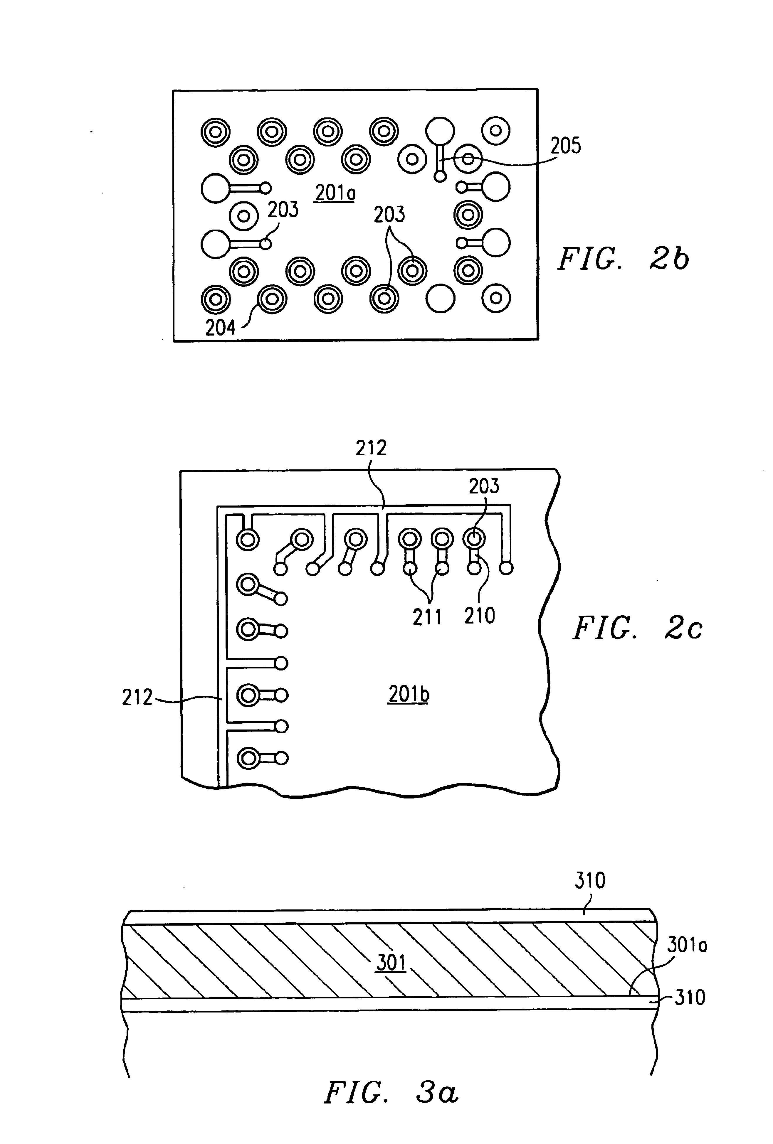
[0028]A typical pattern of solder ball contact pads 204 for a flex circuit package substrate is shown in FIG. 2b. The pads 204 on the second surface 201b of the dielectric film are arrayed in a pattern which will align to and allow contact to be made by solder balls (not shown) to a printed wiring board, or other second level of interconnection. As shown in both FIGS. 2a and 2b, the contact pads 204 are interconnected to the conductive vias 203 by metal traces 205, o...


PUM

PropertyMeasurementUnit
thicknessaaaaaaaaaa
thickaaaaaaaaaa
thickaaaaaaaaaa

Abstract

A method for the fabrication of a double-sided electrical interconnection flexible circuit (200) particularly useful as a substrate for an area array integrated circuit package. A copper matrix with studs (203) is pressed through a dielectric film (201) having a copper layer on the opposite surface, thereby forming an intermediate structure for a flex circuit with self-aligned solid copper vias in a one step process. The contacts are reinforced by plating both surfaces with a layer of copper, and conventional processes are used to complete the circuit patterning.

Description

[0001]This application claims priority under 35 USC § 119 based upon Provisional Patent Application No. 60 / 122,297, filed Mar. 1, 1999.FIELD OF THE INVENTION[0002]The present invention relates generally to flexible circuits and more particularly to a method of fabricating flexible circuits for integrated circuit package interconnections.BRIEF DESCRIPTION OF RELATED ART[0003]As the demand for cheaper, faster and lower power consuming integrated circuits increases, so must the packing density at the circuit board level. Not only have techniques continually evolved to meet the demand for minimizing dimensions of the transistors and of the electrical interconnections which integrate semiconductor devices, but also the packaging technology has advanced resulting in smaller integrated circuit packages with improved electrical and thermal performance.[0004]Ball Grid Array (BGA) and many Chip Scale Packages (CSP) are integrated circuit packages which are assembled to an external circuit boa...

Claims


Application Information

Patent Timeline
Patent Type & Authority Patents(United States)
IPC IPC(8): H01L23/498H01L23/48H05K3/20H05K3/40H05K3/00H05K3/10H05K3/06H05K1/00H01L21/60
CPCH01L23/4985H05K3/205H05K3/207H05K3/4038Y10T29/49165H01L2224/32245H01L2224/48091H01L2224/48247H01L2224/48465H01L2224/73265H01L2924/01078H01L2924/01079H01L2924/30107H05K1/0393H05K3/005H05K3/064H05K3/102H05K3/20H05K2201/09563H05K2201/09981H05K2203/0108H05K2203/0195H05K2203/033H05K2203/0338H05K2203/0369H05K2203/0522H05K2203/1189H01L2224/16Y10T29/49117Y10T29/49167Y10T29/49155Y10T29/49126Y10T29/49156H01L24/48H01L2924/00014H01L2924/00H01L2924/00012H01L2924/12042H01L2924/00015H01L24/73H01L2924/14H01L2924/181H01L2224/85399H01L2224/05599H01L2224/45099H01L2224/45015H01L2924/207
Inventor ABBOTT, DONALD C.COTUGNO, JOHN E.FRITZSCHE, ROBERT M.SABO, ROBERT A.SULLIVAN, CHRISTOPHER M.WEST, DAVID W.
Owner TEXAS INSTR INC
Why Eureka
Try Eureka