Planar coil and planar transformer, and process of fabricating a high-aspect conductive device

a technology of planar coil and conductive device, which is applied in the direction of fixed transformers or mutual inductances, conductive pattern formation, inductance, etc., can solve the problems of increasing the wiring resistance of the primer film, increasing the spacing between conductive patterns, and reducing so as to achieve excellent electric properties, reduce the direct current resistance of the planar coil, and increase the thickness of the conductor

Inactive Publication Date: 2003-07-29
TDK CORPARATION
View PDF6 Cites 92 Cited by
  • Summary
  • Abstract
  • Description
  • Claims
  • Application Information

AI Technical Summary

Benefits of technology

In the planar coil according to the first aspect of the invention, the thickness of the conductor can be increased while the spacing between coil conductive filaments is kept small, so that the direct current resistance of the planar coil can be reduced. This planar coil may be used to construct a planar transformer showing excellent electric properties even when operated with small power of up to 10 W.
The fabrication process according to the second aspect of the invention has the following advantages over a conventional process of fabricating planar coils.
(1) By using as the plating primer film the metal thin film provided all over the surface of the substrate, a large current can be so supplied that a high-aspect pattern can be formed and the given plating thickness can be obtained in one plating operation.
(2) All regions but the plating primer film under the openings in the conductor are covered with the resist, and the plating primer film in relatively thin. Accordingly, even when the conductor spacing is very narrow relative to the conductor height, high throughput can be achieved by wet etching yet at low running cost.
(4) The formed conductor itself can be used for exposure of the inter-conductor primer film for etching purposes. This can dispense with the use of a photomask, and awkward alignment, and so can simplify the fabrication process.
(5) The protective metal layer is usually of a few .mu.m in thickness, and so can be formed within a short time of about 10 minutes immediately upon plating. Thus, the fabrication process can be simplified.

Problems solved by technology

However, a serious problem with such a process is that while the conductive thin film is etched, an etching solution burrows its way into a portion of the conductive thin film covered with the resist pattern, causing removal of the conductor at that portion by dissolution.
This in turn causes the section of the remaining conductor to assume on a trapezoidal shape, resulting in considerable increases in the spacing between conductive patterns.
However, such as when the spiral pattern is especially formed on the conductive thin film that is a plating primer film, there is an increase in the wiring resistance of the primer film because the thickness of the conductive thin film is very small.
This then renders it impossible to increase plating currents, resulting in an unavoidable increase in the length of time needed for plating.
In addition, it is impossible to increase the thickness of the conductive pattern because the growth rate of plating is usually lacking in anisotropy.
To add to this, high-speed plating causes deformation of the resist wall due to its softness; there is no choice but to decrease the working current, with a working efficiency drop.
Moreover, the need of special equipment incurs some extra expenses.
Thus, many problems arise in putting this process to practical use.
When this process is applied to the fabrication of a planar coil, it is difficult to increase the thickness of a coil conductor itself.
In other words, the space factor of a coil conductive portion is too low to achieve favorable electric properties, because direct current resistance increases unavoidably.

Method used


Image

  • Planar coil and planar transformer, and process of fabricating a high-aspect conductive device
  • Planar coil and planar transformer, and process of fabricating a high-aspect conductive device
  • Planar coil and planar transformer, and process of fabricating a high-aspect conductive device

Examples


example 1-1

Examples regarding the first aspect of the invention are given below.

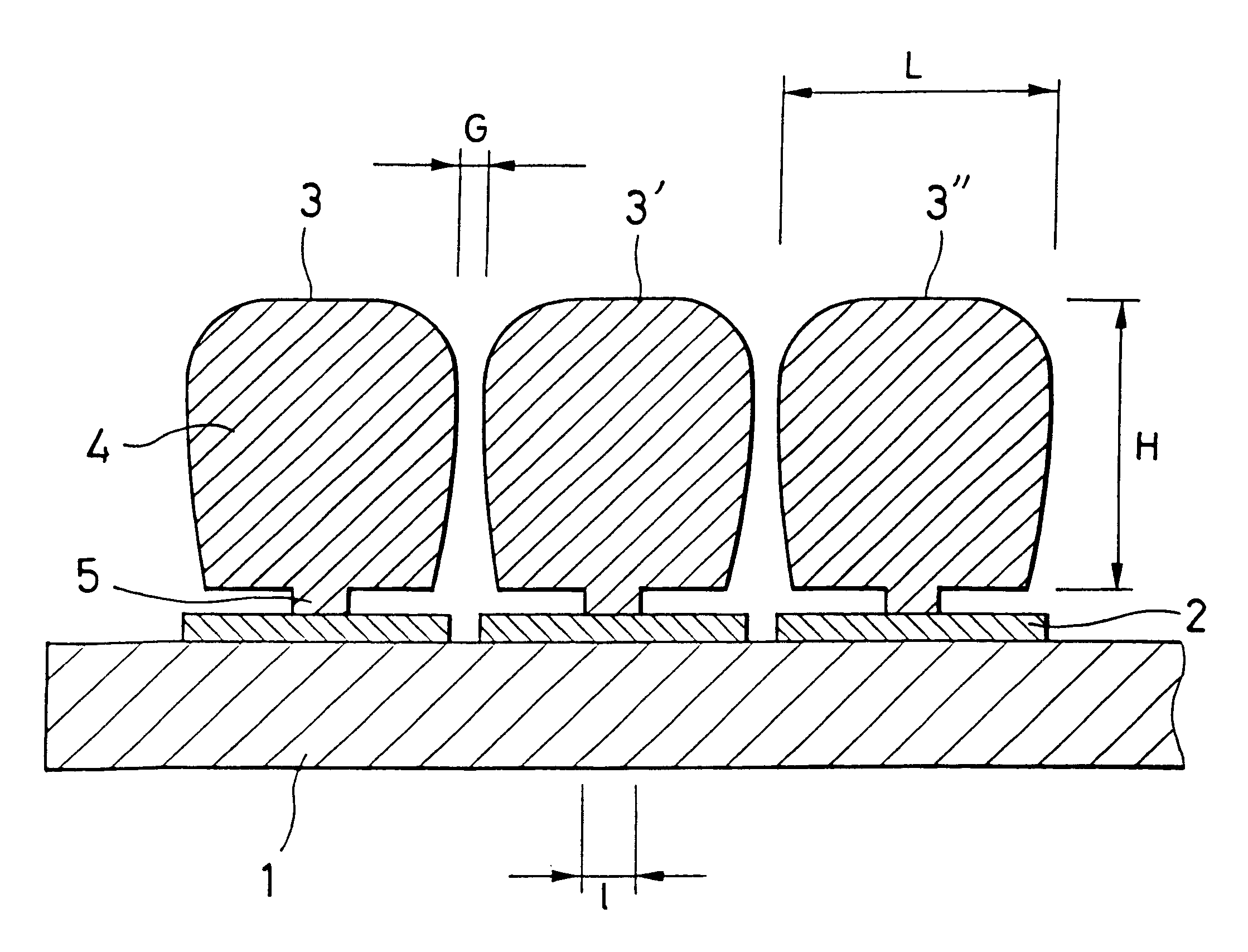
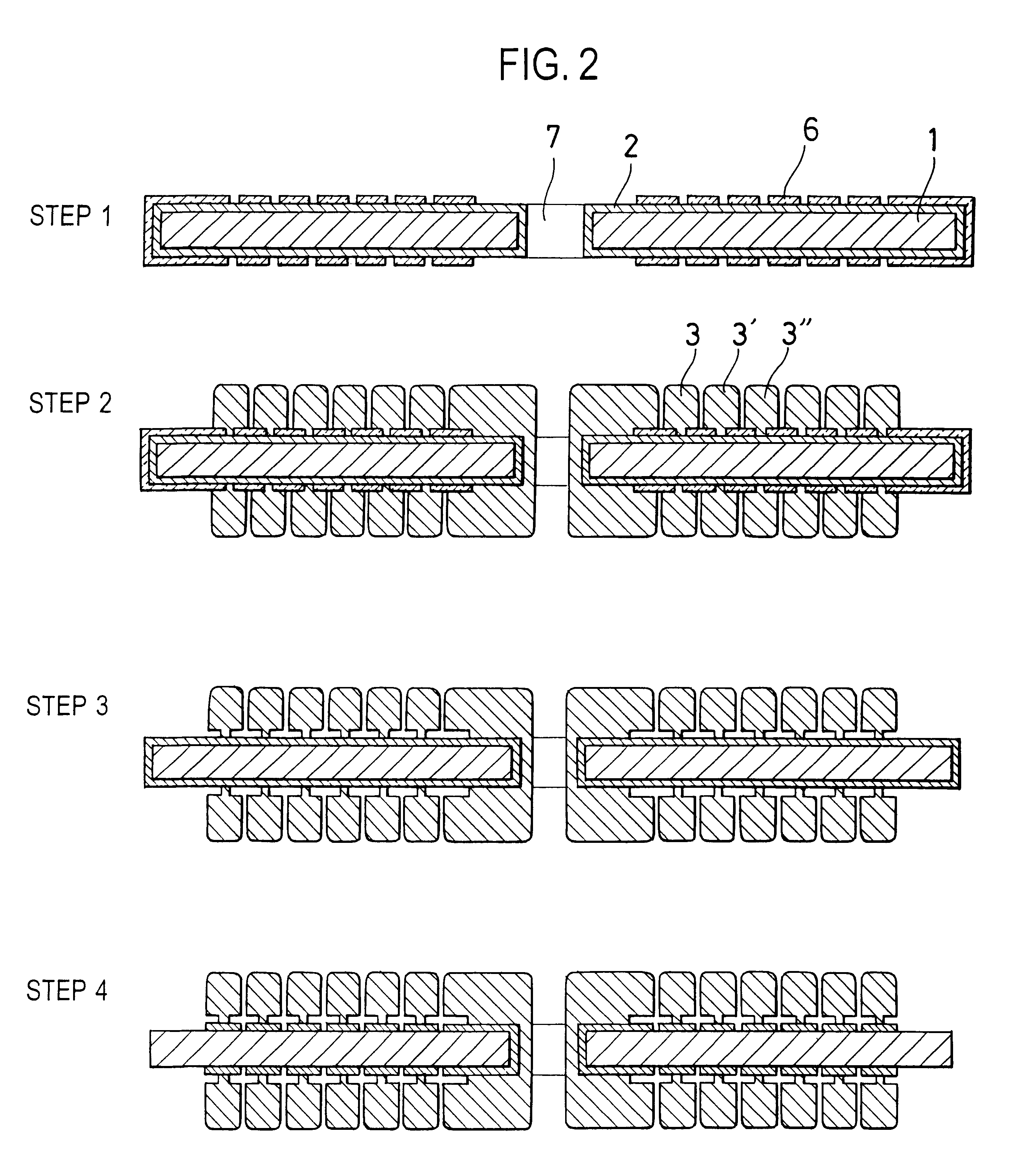
To fabricate 284 coils on a 3-inch substrate, the following operations were carried out. A through-hole of 0.2 mm in diameter was provided through an unclad FR4 substrate (of 100 .mu.m in thickness) at a given position thereof, and 1-.mu.m thick copper layers were formed on both surfaces of the substrate, using an electroless copper plating solution.

A positive photoresist was spin-coated on each copper layer at a dry thickness of 5 .mu.m.

Then, the resist was stripped away from the circumference of the through-hole. At the same time, a pattern having a resist pattern width of 90 .mu.m and a resist pattern spacing (i.e., a line width of the conductor exposed) of 20 .mu.m was provided by photolithography to form a coil portion. The through-hole was provided to make connections between the copper layers on both surfaces of the substrate. A pattern of a portion with the resist stripped away therefrom, i.e., the coil por...

example 1-2

A through-hole of 0.2 mm in diameter was provided through the same unclad FR4 substrate as in Example 1-1 at a given position thereof, and 1-.mu.m thick copper layers were formed on both surfaces of the substrate, using an electroless copper plating solution.

A positive photoresist was spin-coated on each copper layer at a dry thickness of 5 .mu.m, and a pattern having a resist pattern width of 110 .mu.m and a resist pattern spacing (i.e., a line width of the conductor exposed) of 20 .mu.m was provided by photolithography. The through-hole was provided to make connections between the copper layers on both surfaces of the substrate. A pattern of a portion with the resist stripped away therefrom, i.e., a coil portion was in a round spiral form having an innermost radius of 0.9 mm and 9.5 turns.

This was plated in a bright copper sulfate plating bath. The concentration of copper sulfate in a plating solution was 70 g / l, and the plating solution temperature was 25.degree. C. A pipe with a...

example 1-4

An NiZn ferrite substrate having a diameter of 3 inches, a thickness of 350 .mu.m and a relative permeability of 800 was provided on both its surfaces with 1-.mu.m thick copper layers, using an electroless copper plating solution.

A positive photoresist was spin-coated on each copper layer at a dry thickness of 5 .mu.m, and a pattern having a resist pattern width of 90 .mu.m and a resist pattern spacing (i.e., a line width of the conductor exposed) of 20 .mu.m was provided by photolithography. A pattern of a portion with the resist stripped away therefrom, i.e., a coil portion was in a round spiral form having an innermost radius of 0.9 mm and 5.75 turns.

This was plated in a bright copper sulfate plating bath. The concentration of copper sulfate in a plating solution was 70 g / l, and the plating solution temperature was 25.degree. C. Plating was carried out at a current density of 2.5 A / dm.sup.2 as in Example 1-1 until a plating thickness of 150 .mu.m was obtained. At this time, the s...


PUM

PropertyMeasurementUnit
poweraaaaaaaaaa
thicknessaaaaaaaaaa
thicknessaaaaaaaaaa

Abstract

A planar coil including and insulating substrate, and a coil conductive filament having a thickness of 20 to 400 mum and formed on at least one surface of the insulating substrate, the coil conductive filament having a gap whose aspect ratio (H/G) is at least 1. The coil conductive filament has a cross-section in a substantially mushroom shape having a head and a neck, the head has a width (L) which is a least twice as large as a width (l) of the neck thereof, at most 1.5 times as large as a height of the head, and at least twice as large as a minimum spacing (G) between adjacent coil conductive filaments.

Description

The present invention relates generally to a planar coil and a plane transformer, and more particularly to a planar coil and a planar transformer capable of operating with small power of 10 W or less. The present invention is also concerned with a process of fabricating a high-aspect conductive device comprising a plurality of fine yet thick conductive patterns arranged side by side at a narrow spacing, for instance, a planar coil, and a printed circuit board.Planar coils are widely used in the form of biaxial actuators for digital audio disks, and power sources or signal sources for artificial satellites, and fine-pitch printed circuit boards are employed as general-purpose parts of portable terminal equipment, and high-density packaged electronic equipment. Planar coils are also incorporated in thin-film heads.As planar coils, and printed circuit boards capable of functioning as precise devices are now in growing demand, an arrangement comprising a plurality of fine yet thick cond...

Claims


Application Information

Patent Timeline
Patent Type & Authority Patents(United States)
IPC IPC(8): H01F17/00H01F5/00H05K1/02H05K3/10H01F19/00H01F19/04H05K3/06H05K1/16
CPCH01F5/003H01F17/0013H05K1/0265H05K3/108H01F17/0006H01F19/04H05K1/165H05K3/062H05K2201/098
Inventor KAJINO, TAKASHI
Owner TDK CORPARATION
Why Eureka
Try Eureka