Photosensitive composition for manufacturing optical waveguide, production method thereof and polymer optical waveguide pattern formation method using the same

a technology of optical waveguides and compositions, applied in the direction of photosensitive materials, instruments, photomechanical equipment, etc., can solve the problems of substantially complicated construction of optical devices, and achieve the effects of simple pattern formability, superior heat stability and moisture resistance, and small birefringen

Inactive Publication Date: 2005-08-23
NIPPON TELEGRAPH & TELEPHONE CORP
View PDF12 Cites 2 Cited by
  • Summary
  • Abstract
  • Description
  • Claims
  • Application Information

AI Technical Summary

Benefits of technology

[0018]In view of such circumstances relating to a polymer material for an optical waveguide, the present invention relates to a photosensitive composition for producing an optical waveguide and a polymer optical waveguide pattern formation method. The present invention provides an optical waveguide material consisting of a polymer material with a photosensitivity. This invention discloses simple and high-speed waveguide formation with outstanding performance in all of transparency, heat stability, optical isotropy and processability.
[0019]When an aromatic group such as benzene ring is contained in a molecular structure in order to improve the heat stability, the aromatic group such as benzene ring is oriented to manifest an optical anisotropy thereby increasing birefringence. Because an optical waveguide or the like produced using such a material has a polarization dependence, its output characteristic is changed by variation of polarization plane even when the intensity of incident light is constant. In particular, this is a problem when the waveguide is actually used as a single mode optical waveguide. To eliminate the polarization dependence, it is necessary to use in combination with a polarizer. However, this method has a disadvantage because it makes the construction of the optical device substantially complicated.
[0020]The polymer optical waveguide pattern formation method according to the present invention has been made in view of such present circumstances. The object of the present invention is to form a polymer optical waveguide pattern which is simple and suitable for mass production and can be easily connected with optical components by using a reactive oligomer which has simple pattern formation ability, superior heat stability and moisture resistance, small birefringence, and superior processability.

Problems solved by technology

In particular, this is a problem when the waveguide is actually used as a single mode optical waveguide.
However, this method has a disadvantage because it makes the construction of the optical device substantially complicated.

Method used


Image

  • Photosensitive composition for manufacturing optical waveguide, production method thereof and polymer optical waveguide pattern formation method using the same
  • Photosensitive composition for manufacturing optical waveguide, production method thereof and polymer optical waveguide pattern formation method using the same
  • Photosensitive composition for manufacturing optical waveguide, production method thereof and polymer optical waveguide pattern formation method using the same

Examples


example 1

[0061]Phenyltrichlorosilane (211.5 g) and methyltrichlorosilane (36.3 g) were dissolved in 1 liter of anhydrous tetrahydrofuran, and 3 equivalents of water (67.5 g) was slowly added dropwise to the solution so that the liquid temperature does not increase. After that, 315 g of sodium hydrogencarbonate was added while agitating the reaction liquid. After the completion of carbon dioxide gas evolution, agitation was continued for further 1 hour. Next, the reaction liquid was filtered, then tetrahydrofuran was distilled out by a rotary evaporator to give a colorless, transparent viscous liquid. Further, this liquid was vacuum dried to give an oligomer A. The molecular weight of resulting oligomer A was measured by GPC and the result was Mw=3300, Mn=1500.

[0062]Next, a photosensitive substance A was prepared which comprises 50 g of oligomer A, 25 g of UV resin, 2 weight % of N-benzyl-4-benzoylpyridinium hexafluoroantimonate as a photopolymerization initiator and 25 g of methylisobutylket...

example 2

[0064]A photosensitive substance B was prepared which comprises 50 g of the oligomer A produced in Example 1, 1 g of (3-glycidoxypropyl)trimethoxysilane as a crosslinking agent, 2 weight % of N-benzyl-4-benzoylpyridinium hexafluoroantimonate as a photopolymerization initiator, and 25 g of methylisobutylketone as a solvent.

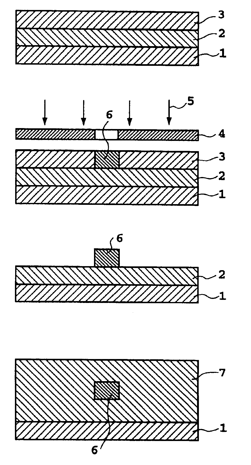
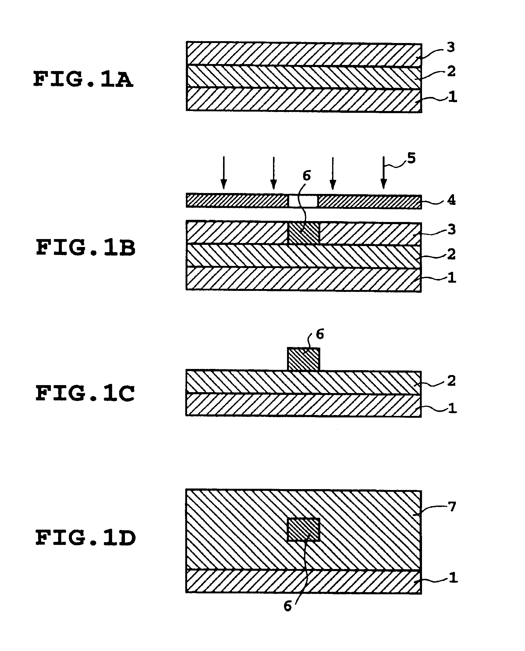
[0065]Using the same procedure as in Example 1 except that the photosensitive substance B was used in place of the photosensitive substance A as a core part forming photosensitive substance, a buried type channel optical waveguide comprising a core-clad layer structure as shown in FIG. 1D was produced. In this case, the thickness of the upper clad is 8 μm from the upper surface of the core. Further, no intermixing was noted between the lower clad layer and the core part formation layer.

[0066]As in Example 1, the resulting optical waveguide was cut to a length of 5 cm by a dicing saw, and measured for optical propagation loss which showed 0.5 dB / cm at wavelength 1.3...

example 3

[0067]Oligomer B was produced using the same procedure as in Example 1 except that deuterated phenyltrichlorosilane was used in place of phenyltrichlorosilane in the production of oligomer A in Example 1, and a photosensitive substance C was produced using the same procedure as in Example 2 except that oligomer B was used in place of oligomer A. Next, a buried type channel optical waveguide of core diameter 8 μm×8 μm was produced by the same process as in Example 2.

[0068]The resulting optical waveguide was cut to a length of 5 cm by a dicing saw, and measured for optical propagation loss which showed 0.1 dB / cm at wavelength 1.3 μm, and 0.5 dB / cm or less at wavelength 1.55 μm. Further, this optical propagation loss of the waveguide was unchanged for more than 1 month under the condition of 75° C. / 90% RH.


PUM

PropertyMeasurementUnit
thicknessaaaaaaaaaa
thicknessaaaaaaaaaa
widthaaaaaaaaaa

Abstract

A photosensitive composition for optical waveguides comprising of an organic oligomer, a polymerization initiator and a crosslinking agent, the organic oligomer being a silicone oligomer represented by the following formula (1), wherein X denotes hydrogen, deuterium, halogen, an alkyl group or an alkoxy group; m is an integer from 1 to 5; x and y represent the proportion of respective units, and neither x nor y is 0; and R1 denotes a methyl, ethyl, or isopropyl group; a production method thereof, and a polymer optical waveguide pattern formation method using the same.

Description

CROSS REFERENCE TO RELATED APPLICATION[0001]The present application is a divisional of U.S. patent application Ser. No. 10 / 262,777, filed on Oct. 2, 2002 now U.S. Pat. No. 6,806,040, which is a divisional of U.S. patent application Ser. No. 09 / 409,078, filed Sep. 30, 1999, now U.S. Pat. No. 6,537,723 the contents of which are incorporated in their entirety herein.[0002]This application is based on Patent Application No. 10-283142 filed on Oct. 5, 1998 in Japan, the content of which is incorporated hereinto by reference.BACKGROUND OF THE INVENTION[0003]1. Field of the Invention[0004]The present invention relates to a polymer optical waveguide pattern formation method using a polymer material. The present invention can be utilized in various optical waveguides, optical integrated circuits, optical wiring boards and the like which are used in general optical and micro-optical areas and in optical communication or optical information processing areas.[0005]2. Description of the Related ...

Claims


Application Information

Patent Timeline
Patent Type & Authority Patents(United States)
IPC IPC(8): G03F7/075G03F7/038
CPCG03F7/0757G03F7/038Y10S430/117Y10S430/106Y10S430/115
Inventor TOYODA, SEIJIIMAMURA, SABUROTOMARU, SATORUKURIHARA, TAKASHIENBUTSU, KOJIHAYASHIDA, SHOICHIMARUNO, TOHRU
Owner NIPPON TELEGRAPH & TELEPHONE CORP
Why Eureka
Try Eureka