Boron phosphide-based semiconductor light-emitting device, production method thereof and light-emitting diode

Inactive Publication Date: 2005-08-30
SHOWA DENKO KK
View PDF16 Cites 18 Cited by
  • Summary
  • Abstract
  • Description
  • Claims
  • Application Information

AI Technical Summary

Benefits of technology

[0014]However, as in the aforementioned conventional technique, the suitable vapor phase growth temperature for forming a well layer included in the light-emitting layer having a quantum well structure greatly differs from that for forming a p-type boron phosphide layer. Therefore, when the p-type boron phosphide layer is vapor-phase grown at high temperature, variation in indium content in an indium-containing nitride semiconductor layer serving as the well layer is induced. The variation in indium content means generally a decrease in indium content, which reduces stability of quan

Problems solved by technology

In order to produce a light-emitting device operable at a lowered forward voltage (Vf) or a reduced threshold voltage (Vth), a technique for forming a low contact resistance Ohmic electrode is also a critical issue.
With regard to a p-side-up type light-emitting device, a particularly essential issue is the method of forming a p-type Ohmic electrode so as to attain contact with a low-resistive p-type conduction layer.
The variation in indium content means generally a decrease in indium content, which reduces stability of quantum levels in the well layer.
The decrease in stability disturbs successful production of a boron phosphide-based semiconductor light-emitting device for emitting light of excellent monochromaticity having a narrow

Method used


Image

  • Boron phosphide-based semiconductor light-emitting device, production method thereof and light-emitting diode
  • Boron phosphide-based semiconductor light-emitting device, production method thereof and light-emitting diode
  • Boron phosphide-based semiconductor light-emitting device, production method thereof and light-emitting diode

Examples


example 1

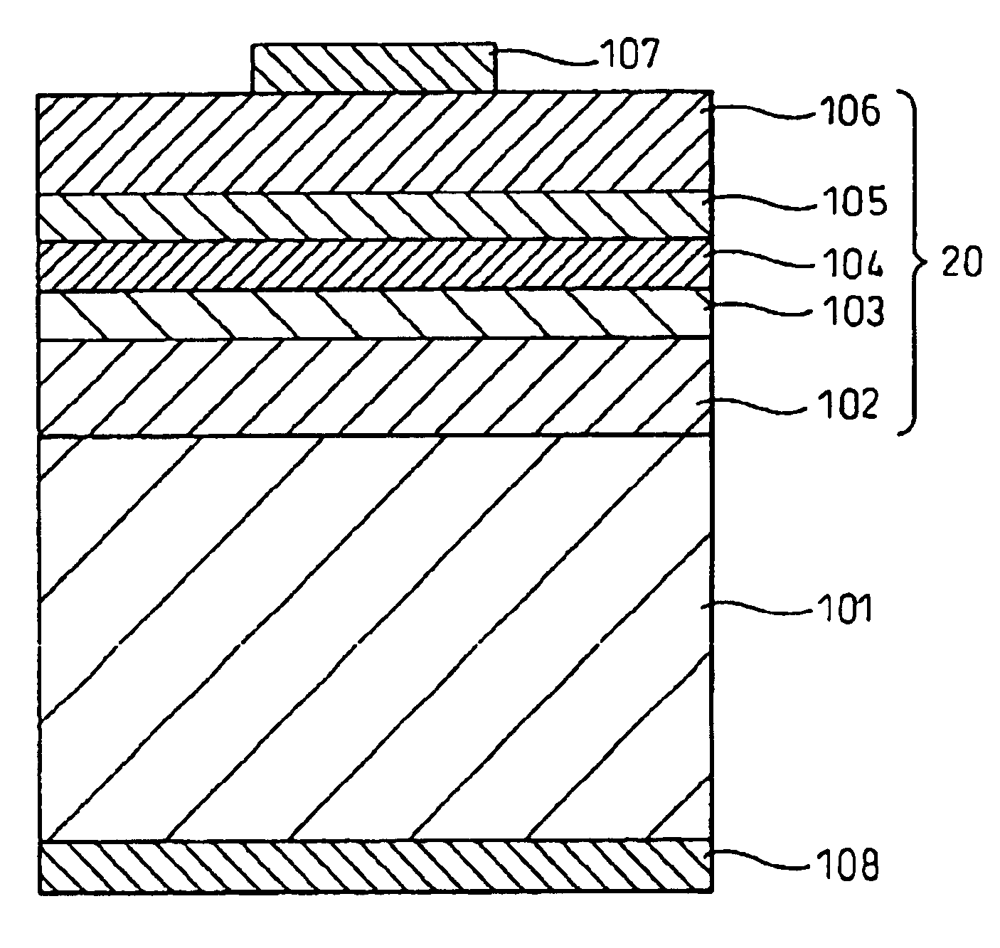
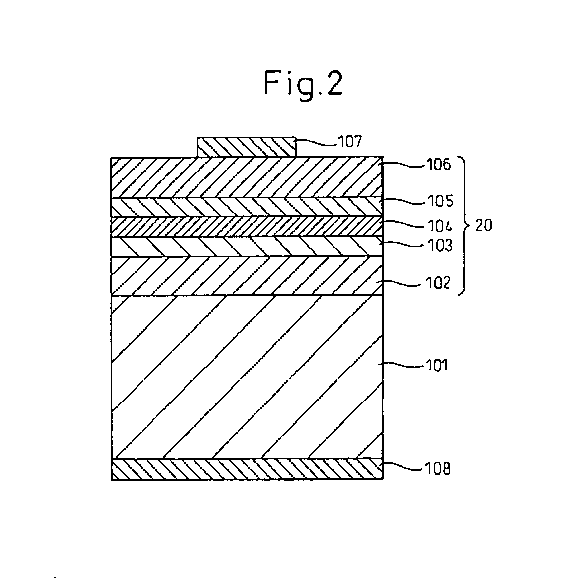
[0101]A double-hetero-junction light-emitting diode (LED) having a pn-junction structure including an upper cladding layer formed of p-type boron phosphide and a light-emitting layer formed of n-type gallium nitride was produced as an exemplary boron phosphide-based semiconductor light-emitting device. FIG. 2 schematically shows a cross-section of the produced LED.

[0102]A phosphorus (P)-doped n-type silicon {111} single crystal was used as a single-crystal substrate 101. Firstly, on the {111} surface of the single-crystal substrate 101, a lower cladding layer 102 formed of an undoped n-type boron phosphide layer was vapor-phase grown through atmospheric-pressure (near atmospheric pressure) MOCVD at 925° C. by use of a triethylborane ((C2H5)3B) / phosphine (PH3) / hydrogen (H2) system. The n-type boron phosphide layer serving as the lower cladding layer 102 was formed at a concentration ratio regarding sources fed to a vapor phase growth zone; i.e., a V / III ratio (═PH3 / (C2H5)3B ratio) of...

example 2

[0121]The boron phosphide-based compound semiconductor device according to the present invention will next be described in detail, taking as an example a light-emitting diode (LED) employing a boron phosphide (BP) amorphous layer, which is a typical boron phosphide-based semiconductor.

[0122]FIG. 3 schematically shows the cross-section of a stacked structure 13 employed for fabricating an LED 12 having a pn-junction type double-hetero (DH) structure. FIG. 4 is a schematic plane view of the LED shown in FIG. 3.

[0123]A (0001)-sapphire (α-Al2O3 single crystal) was used as a single-crystal substrate 101. On the (0001)-surface of the single-crystal substrate 101, a lower cladding layer 102 formed of n-type gallium nitride (GaN) was deposited through atmospheric pressure (near atmospheric pressure) metal-organic vapor phase epitaxy (MOVPE) means. The lower cladding layer 102 was deposited at 1,050° C. by use of a trimethylgallium (molecular formula: (CH3)3Ga) as a gallium (Ga) source and a...

example 3

[0132]FIG. 5 is a schematic cross-sectional view of an LED 30 mentioned in this Example. FIG. 6 is a schematic plane view of the LED 30. The cross-section of FIG. 5 is a cross-section along the broken line A-A′ shown in FIG. 6. A phosphorus (P)-doped n-type (111)-Si single crystal was used as a single-crystal substrate 301. Firstly, on the (111)-surface of the single-crystal substrate 301, a lower cladding layer 302 formed of undoped n-type monomeric boron phosphide (BP) was deposited through atmospheric pressure (near atmospheric pressure) metal-organic chemical vapor deposition (MOCVD) means. The n-type lower cladding layer 302 was formed at 950° C. by use of a triethylborane (molecular formula: (C2H5)3B) / phosphine (molecular formula: PH3) / hydrogen (H2) reaction system. The thickness of the n-type lower cladding layer 302 was controlled to 240 nm so as to attain a reflectance of 40% or higher within a blue light wavelength range of 430 nm to 460 nm. Feeding of the aforementioned b...


PUM

PropertyMeasurementUnit
Temperatureaaaaaaaaaa

Abstract

A boron phosphide-based semiconductor light-emitting device, which device includes a light-emitting member having a hetero-junction structure in which an n-type lower cladding layer formed of an n-type compound semiconductor, an n-type light-emitting layer formed of an n-type Group III nitride semiconductor, and a p-type upper cladding layer provided on the light-emitting layer and formed of a p-type boron phosphide-based semiconductor are sequentially provided on a surface of a conductive or high-resistive single-crystal substrate and which device includes a p-type Ohmic electrode provided so as to achieve contact with the p-type upper cladding layer, characterized in that a amorphous layer formed of boron phosphide-based semiconductor is disposed between the p-type upper cladding layer and the n-type light-emitting layer. This boron phosphide-based semiconductor light-emitting device exhibits a low forward voltage or threshold value and has excellent reverse breakdown voltage characteristics.

Description

CROSS-REFERENCE TO RELATED APPLICATIONS[0001]This application is an application filed under 35 U.S.C. §111(a) claiming benefit pursuant to 35 U.S.C. §119(e)(1) of the filing date of Provisional Applications No. 60 / 428,716 filed Nov. 25, 2002, No. 60 / 436,640 filed Dec. 30, 2002 and No. 60 / 436,641 filed Dec. 30, 2002, pursuant to 35 U.S.C. §111(b).BACKGROUND OF THE INVENTION[0002]1. Field of the Invention[0003]The present invention relates to a boron phosphide-based semiconductor light-emitting device and to a method for producing the same. More particularly, the invention relates to a boron phosphide-based semiconductor light-emitting device exhibiting a low forward voltage or threshold voltage, having excellent reverse breakdown voltage characteristics, having a high emission intensity, and having a small decrease in emission intensity caused by long-term passage of device operation current. Furthermore, the invention relates to a method for producing the boron phosphide-based semic...

Claims


Application Information

Patent Timeline
IPC IPC(8): C23C16/30H01L33/00H01L33/02H01L33/16H01L33/30H01L33/32
CPCC23C16/30H01L33/02H01L33/30H01L33/32H01L33/16H01L2924/0002H01L2924/00
Inventor UDAGAWA, TAKASHIKASAHARA, AKIRA
Owner SHOWA DENKO KK
Why Eureka
Try Eureka