Electro-optic displays, and methods for driving same

a technology of optical displays and optical components, applied in the field of optical displays, can solve the problems of affecting the performance of optical displays, requiring a significant amount of power, space, and electronics, and reducing the light degradation of redox chromophores, so as to reduce or eliminate the exposure of the electrochromic active layer, stop or minimize the degradation of electrolytes, and reduce or eliminate the light degradation of the redox chromophore

Inactive Publication Date: 2005-09-27
E INK CORPORATION
View PDF126 Cites 936 Cited by
  • Summary
  • Abstract
  • Description
  • Claims
  • Application Information

AI Technical Summary

Benefits of technology

[0100]The third aspect of the present invention provides an electrochromic display, of the type described in the aforementioned U.S. Pat. No. 6,301,038, WO 01 / 27690 or Wood article, and comprising a nano-porous-nano-crystalline film comprising a semiconducting metal oxide having an electroactive compound which is either a p-type or n-type redox promoter or p-type or n-type redox chromophore adsorbed thereon or otherwise attached thereto, the display having light sealing means arranged to reduce or eliminate exposure of the electrochromically-active layer to radiation, thereby reducing or eliminating the light degradation of the redox chromophore due to photocatalytic reactions at the electrochromically-active layer.
[0101]The third aspect of the present invention also provides an electrochromic display of this type having oxygen sealing and / or removing (“getting”) means for providing an oxygen seal and / or for removing oxygen from within the display in order to stop or minimize the degradation of the electrolyte due to exposure of the electrolyte to oxygen.
[0102]The third aspect of the present invention also provides an electrochromic display of this type having water sealing and / or removing (“getting”) means for providing a water seal and / or for removing water from within the display in order to stop or minimize the degradation of the electrolyte due to exposure of the electrolyte to water.
[0105]The present invention also provides an electrochromic display of this type having means to control the distance between the electrode surfaces of the display to minimize or eliminate high fields, thus removing or reducing the tendency of such high fields to degrade the electrolyte and / or electrochromically-active layer of the display.

Problems solved by technology

The first electro-optic displays, including Nixie-tubes, were expensive and fragile, were severely limited in the data they could present, and required a significant amount of power, space, and support electronics.
This hampered both their usefulness and acceptance.
Control circuitry was easily implemented with existing digital circuit techniques but still required high power drive stages.
Since LED's still drew a significant amount of power and could not easily scale to meet the increasing market demand for higher resolution displays, display development moved to new approaches.
The passive-matrix system is simple and cost effective, but it has significant drawbacks, notably slow response time and imprecise voltage control.
In addition, imprecise voltage control hinders the passive matrix's ability to influence only one pixel at a time.
When voltage is applied to untwist one pixel, the pixels around it also partially untwist, which makes images appear fuzzy.
When different levels of twist are required, i.e., gray scale, control of the applied voltage level is required, necessitating more complex drive circuitry and knowledge of the optical properties versus voltage curve.
The liquid crystal-based electro-optic display industry has been subject to the same cost / performance market pressure as the microelectronics industry.
However, LCD's do have some inherent drawbacks.
Transmissive LCD's require backlighting, which draws significant power.
Also, the contrast, though much improved over early implementations, is inherently limited to the background and foreground colors and color differentiation.
Reflective LCD's (which essentially place a reflector on the opposed side of the display from the observer) have insufficient contrast for many applications.
Furthermore, since the extent of rotation of the plane of polarization of light by the liquid crystal depends upon the thickness of liquid crystal layer, this thickness must be accurately maintained, which renders it very difficult to prepare LCD's on flexible substrates.
The OLED technology has shown great potential but limited commercial viability, due to some significant performance issues.
However, the electrical requirements of the OLED pixel circuit are significantly different.
However, many technological challenges lie ahead before OLED's can become a commercially viable display technology; these challenges include short operational life and susceptibility to moisture, which degrades the displays, and requires the use of special hermetically sealed packages.
This type of packaging increases the cost of the overall displays and severely limits the use of these displays, since the hermetically sealed packing is difficult to scale down in thickness and therefore is not useable for very thin display devices (credit card type displays, flexible displays, etc.).
It is also difficult to scale OLED displays to large sizes because of high defect densities and the technical difficulties associated with making OLED's in large area form factors.
Nevertheless, problems with the long-term image quality of electrophoretic displays such as those described in the three aforementioned patents have prevented their widespread usage.
For example, the dispersed particles used in electrophoretic displays tend to settle, resulting in inadequate service-life for these displays.
However, use of optically flat metal oxide layers requires bulk intercalation of ions as the surface area in contact with electrolyte is not significantly larger than the geometric area.
However, despite the rapid switching times in such films, the associated change in transmittance is not sufficient for a commercial device.
This step is expensive and can lead to product defects if the seal leaks, which is possible with changes in temperature (temperature cycling).
When the cells are close together, ion transport of one cell can create ion transport of neighboring cells and therefore can cause the neighboring non-activated cells to become somewhat activated, resulting in a loss of clarity or resolution.
Currently electrochromic displays are limited in contrast, because although the redox chromophores change color when ion transport occurs, they do so against a clear electrolyte, and a thin (3-4 μm) roughened surface, which is not optimized for contrast, since it is chosen to enhance the amount of surface area for the connection of redox chromophore and not for particular optical properties.
Currently, electrochromic display manufacturing processes are time consuming (>12 hours of preparation time) and therefore are costly.
In addition, because of the high-temperature (450° C.) titania sintering step, these processes do not integrate well with low-temperature plastic-based processes for producing flexible displays.
Application of electrochromic media in VT windows will necessarily expose the media to substantial variations in environmental conditions, and in the present state of electrochromic technology, the applications of electrochromic media are, the present inventors have realized, significantly limited by the susceptibility of such media to many environmental factors, such as light, moisture, oxygen, and electrostatic discharge.
One major limitation of electrochromic media, the present inventors have realized, is the susceptibility of the redox chromophore to light degradation.
Another problem with electrochromic media, the present inventors have realized, is their susceptibility to damage by discharges of static electricity, such as triboelectric charges built up during assembly of a display or its handling as it is moved to a desired location.
Static discharges can damage electronic parts and affect components of the media, especially where the discharge passes through interfaces.
Although the exact reactions involved are not completely understood, exposure of electrochromic media to large “over potentials” beyond the working voltage of the media can degrade the redox chromophore by oxidation or reduction.
Another possible problem with electrochromic media, the present inventors have realized, is interaction between pixels.
Another problem with electrochromic media, the present inventors have realized, is high fields caused by a lack of height or distance control within an electrochromic display between the glass substrates, for example as shown in FIG. 1.
Hence, the electrodes and other components of the display can degrade due to arcing, shorting, or excessive ion transport.
Indeed, it is not quite clear how to make active matrix nano-crystalline electrochromic displays since a common electrolyte that is used between cells may cause interference between cells in an active matrix.
Even in direct-drive nano-crystalline electrochromic displays, the system (electronics / software / display) and method of operation are complex because, as in the electrophoretic display cell discussed earlier, the state of the cell before it is written is critical in determining how to change the cell state.
Thus, using a fixed drive pulse with an encapsulated electrophoretic medium which is undergoing changes in ambient temperature and humidity, and is also aging, can lead to substantial and undesirable changes in the optical properties of the medium.
For example, the medium may show acceptable properties when switched at room temperature, but its contrast ratio may be reduced when operating at low temperatures, and the medium may be over-saturated and / or over-driven at high temperatures; such over-driving is undesirable because it tends to reduce the working lifetime of the medium.
Changes in environmental conditions may also cause problems with self-erasing of the medium.
Obviously, self-erasing is highly undesirable in that it reverses (or otherwise distorts, in the case of a grayscale medium) the desired optical state of the medium.
Similar problems are encountered with other types of electro-optic media.

Method used


Image

  • Electro-optic displays, and methods for driving same
  • Electro-optic displays, and methods for driving same
  • Electro-optic displays, and methods for driving same

Examples


first embodiment

[0163]Section A1: Solid Charge Transport Layer

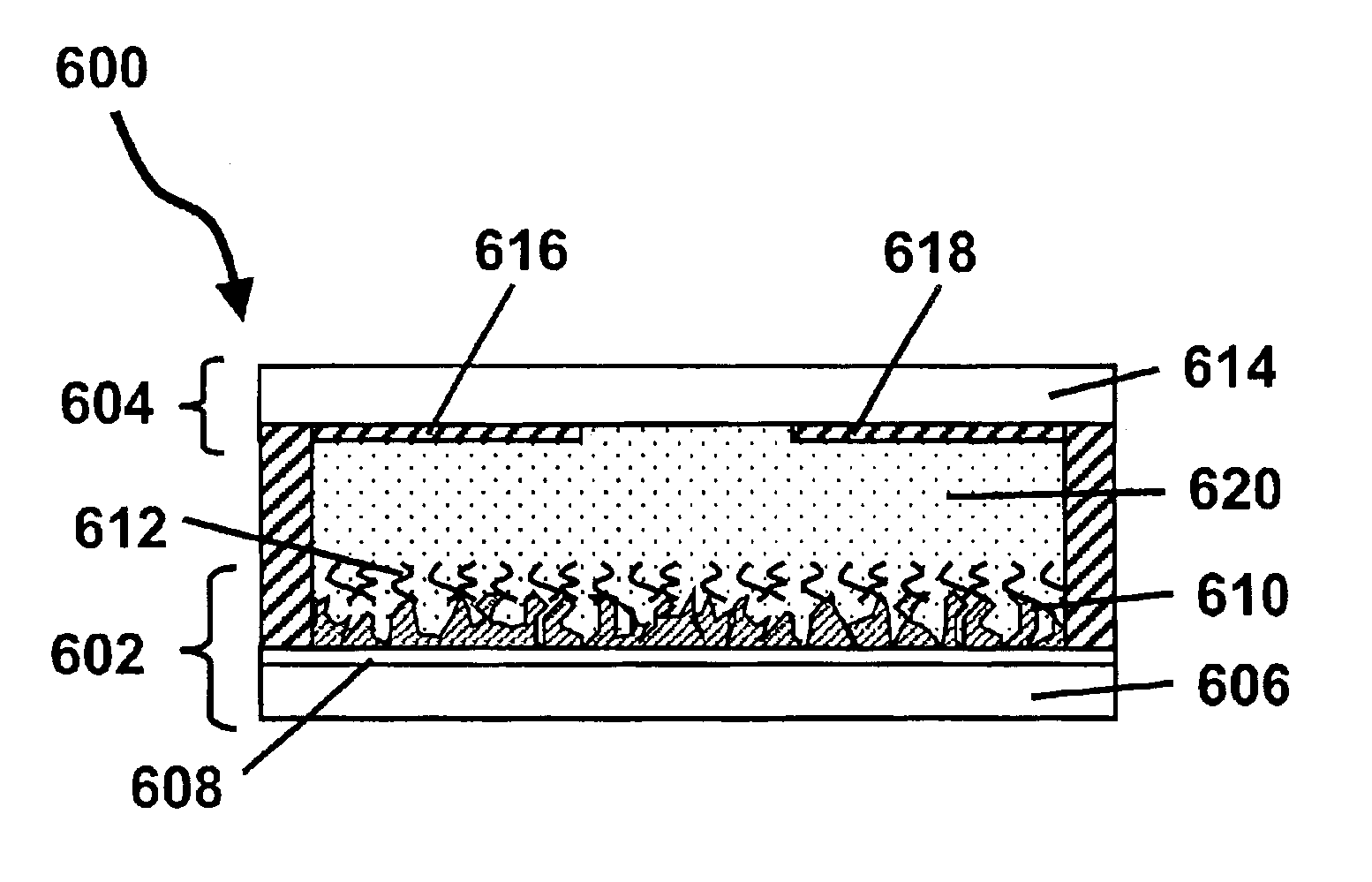
[0164]FIG. 6 shows a schematic cross-section through a display (generally designated 600) having a front section 602 (through which an observer typically views the display 600) and a rear section604. As in the prior art described above, the front section 602 includes a first glass substrate 606, an ITO conductive layer 608, a titania nano-crystalline layer 610, and a redox chromophore (or promoter) layer (e.g., viologen) 612. The rear section 604 includes a second glass substrate 614, and transparent conductive ITO display elements 616 and 618. Not shown are electrical terminals that attach to the conductive layer 608 and to conductive display elements 616 and 618.

[0165]The display 600 further includes, in accordance with the first aspect of the present invention, a solid charge transport layer 620, comprising, for example triphenylamine, which acts in place of the prior art electrolyte between front section 602 and rear section 604, and...

second embodiment

[0174]Section A2: Charge Transport Material Bonded to Promoter or Chromophore

[0175]In the second embodiment of the first aspect of the present invention, a charge transport material is bonded to the redox promoter or chromophore.

[0176]Although other methods of bonding the charge transport material to the redox promoter or chromophore may be used if desired, in a preferred form of the second embodiment, the redox promoter or chromophore is first modified to contain an amino group, if such a group is not already present. The amino-containing promoter or chromophore is then reacted with a charge transport material containing (or modified to contain) an aldehyde, acyl halide or carboxylic acid group to produce a product in which the promoter or chromophore is linked via an amide linkage to the charge transport material.

[0177]Alternatively, the promoter or chromophore may be linked to the charge transport material via an ether linkage, for example by a Williamson ether coupling reaction...

third embodiment

[0180]Section A3: Defined Regions in the Solid Charge Transport Layer

[0181]As already mentioned, the third embodiment of the first aspect of the present invention relates to the use of defined (separate) regions in a solid charge transport layer, and in particular the use of a solid charge transport layer which is interrupted between adjacent pixels of the display. FIG. 8 shows a display (generally designated 800), which is generally similar to the display 600 shown in FIG. 6; in particular, the display 800 comprises glass substrates 606 and 614, an ITO conductive layer 608, a titania nano-crystalline layer 610, a redox chromophore layer 612 and display elements 616 and 618, all of which are essentially the same as the corresponding elements in the display 600 shown in FIG. 6. The display 800 further comprises a solid charge transport layer 820, which is generally similar to the corresponding charge transport layer 620 shown in FIG. 6, but which differs therefrom by being interrupte...


PUM

PropertyMeasurementUnit
diameteraaaaaaaaaa
diameteraaaaaaaaaa
diameteraaaaaaaaaa

Abstract

The invention relates to electro-optic displays and methods for driving such displays. The invention provides (i) electrochromic displays with solid charge transport layers; (ii) apparatus and methods for improving the contrast and reducing the cost of electrochromic displays; (iii) apparatus and methods for sealing electrochromic displays from the outside environment and preventing ingress of contaminants into such a display; and (iv) methods for adjusting the driving of electro-optic displays to allow for environmental and operating parameters.

Description

CROSS REFERENCE TO RELATED APPLICATIONS[0001]This application claims priority from the following Provisional Applications: (a) Ser. Nos. 60 / 365,365; 60 / 365,368; 60 / 365,369; and Ser. No. 60 / 365,385, all of which were filed Mar. 18, 2002; (b) Ser. Nos. 60 / 319,279; 60 / 319,280; and Ser. No. 60 / 319,281, all of which were filed May 31, 2002; and (c) Ser. No. 60 / 319,438, filed Jul. 31, 2002. The entire contents of the aforementioned applications are herein incorporated by reference. The entire contents of all patents and published applications mentioned hereinafter are also incorporated herein by reference.BACKGROUND OF INVENTION[0002]The present invention relates to electro-optic displays and methods for driving such displays. Certain aspects of the present invention are directed especially to electrochromic displays, and more specifically to (i) electrochromic displays with solid charge transport layers; (ii) apparatus and methods for improving the contrast and reducing the cost of elect...

Claims


Application Information

Patent Timeline
Patent Type & Authority Patents(United States)
IPC IPC(8): G02F1/01G02F1/15G02F1/1516
CPCG02F1/15G02F1/1521G02F2201/42G02F1/1503G02F1/1516
Inventor ABRAMSON, JUSTINAMUNDSON, KARL R.DANNER, GUY M.DUTHALER, GREGG M.GATES, HOLLY G.HONEYMAN, CHARLES H.KNAIAN, ARA N.MORRISON, IAN D.O'NEIL, STEVEN J.PAOLINI, JR., RICHARD J.PULLEN, ANTHONY EDWARDWANG, JIANNAZALESKY, JONATHAN L.ZEHNER, ROBERT W.CRONIN, JOHN EDWARD
Owner E INK CORPORATION
Why Eureka
Try Eureka