Method of making a memory structure having a multilayered contact and a storage capacitor with a composite dielectric layer of crystalized niobium pentoxide and tantalum pentoxide films

a multi-layered contact and storage capacitor technology, which is applied in the direction of coatings, transistors, chemical vapor deposition coatings, etc., can solve the problems of affecting the electrical conductivity of the capacitor, and causing the capacitor to fail to meet the requirements of the application. , to achieve the effect of reducing the crystallization temperature, and reducing the leakage curren

Inactive Publication Date: 2005-10-18
RENESAS ELECTRONICS CORP
View PDF7 Cites 3 Cited by
  • Summary
  • Abstract
  • Description
  • Claims
  • Application Information

AI Technical Summary

Benefits of technology

[0032]According to the first and second aspects, it is possible to lower the crystallization temperature, prevent the bottom electrode and the barrier metal from being oxidized, and decrease the leakage current. However, the first aspect is superior to the second aspect in the decrease in the leakage current since the tantalum pentoxide film causing a smaller leakage current is used as the dielectric film. The second aspect is superior to the first aspect in easiness of production of a semiconductor device and a decrease in costs for the following reason: The respective dielectric films constituting the lamination are made of the same material; therefore, it is unnecessary to set separately a means for supplying a source gas for forming the niobium pentoxide film and a means for supplying a source gas for forming the tantalum pentoxide film, or handle the two different source gases for the layered film.
[0033]Subject matters common to the first and second aspects of the present invention are as follows: The dielectric film of a capacitor is made of a bi- or multi-layered insulator, thereby separating the crystal boundaries therein; and the lower dielectric layer of the capacitor is made into a layer comprising niobium pentoxide and the upper dielectric layer is made into a tantalum pentoxide layer, a niobium pentoxide layer, or a layer made of a composition of tantalum pentoxide and niobium pentoxide, whereby the crystallization temperature of the dielectric film can be made lower than that of a tantalum pentoxide film. As a result, the bottom electrode and the barrier metal of the capacitor can be prevented from being oxidized so that the capacitor can be formed as a capacitor having a good leakage current property.
[0034]An example of this capacitor includes a capacitor having a dielectric film composed of a lower layer made of a composition of tantalum pentoxide and niobium pentoxide and an upper layer made of niobium pentoxide. In the case of this capaci

Problems solved by technology

If the plug reacts with the bottom electrode, a bad effect is produced on electrical conductivity.
The problem of the drop in the capacitor capacitance is also generated in the case of forming a silicon nitride film on the surface of the bottom electrode to prevent oxidation of silicon.
As a result, the electrical conductivity thereof is damaged.
Even if the oxidation temperature in the h

Method used


Image

  • Method of making a memory structure having a multilayered contact and a storage capacitor with a composite dielectric layer of crystalized niobium pentoxide and tantalum pentoxide films
  • Method of making a memory structure having a multilayered contact and a storage capacitor with a composite dielectric layer of crystalized niobium pentoxide and tantalum pentoxide films
  • Method of making a memory structure having a multilayered contact and a storage capacitor with a composite dielectric layer of crystalized niobium pentoxide and tantalum pentoxide films

Examples


embodiment 1

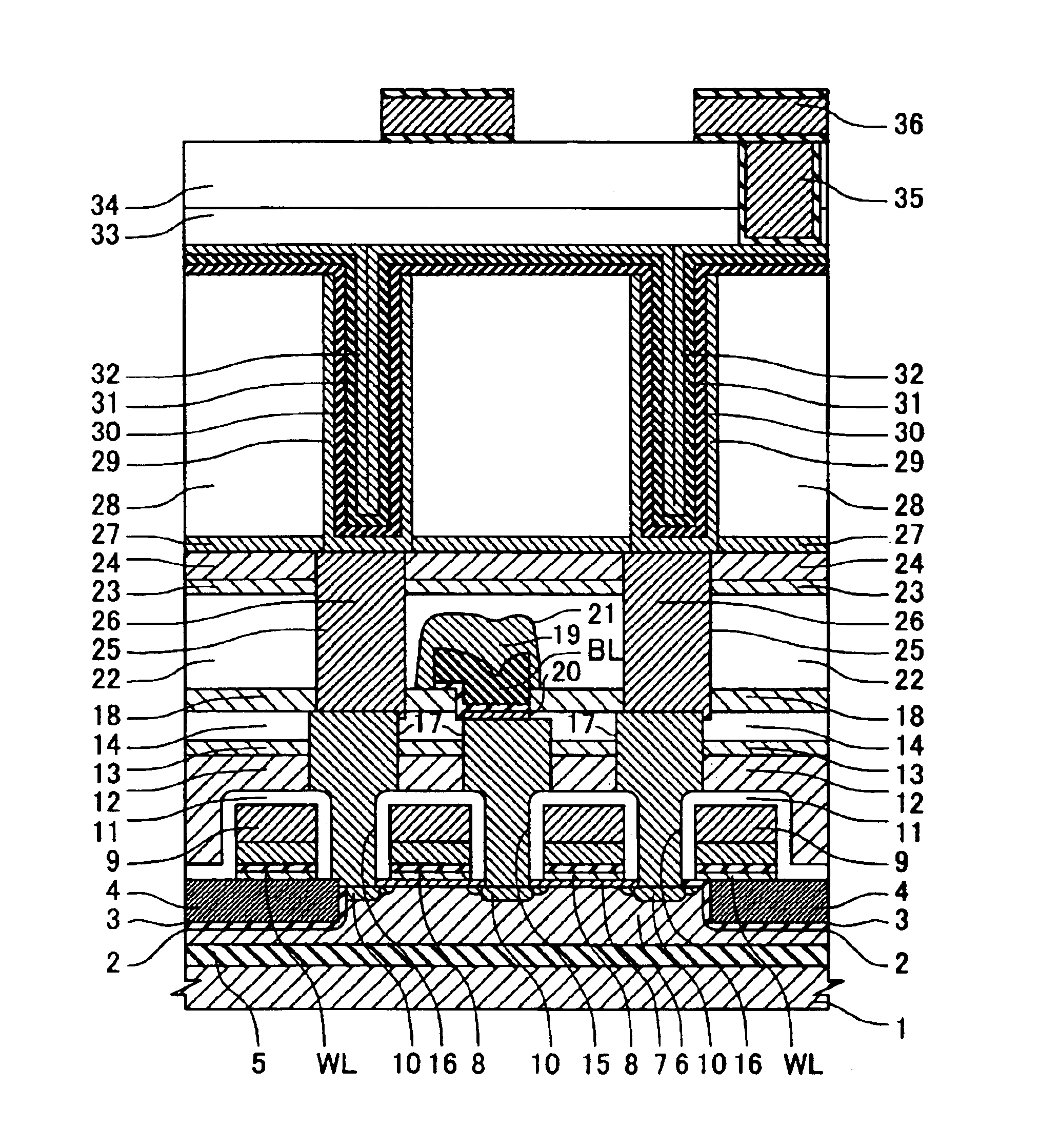
[0053]Referring to FIG. 1, Embodiment 1 of the present invention will be described. This is an embodiment wherein the present invention is applied to a semiconductor memory device having a MIM capacitor using a dielectric film made of a layered film composed of a niobium pentoxide film and a tantalum pentoxide film, in particular, such a DRAM.

[0054]A process for producing the DRAW will be described.

[0055]FIG. 1 is a sectional view of the DRAW to which a capacitor of the present invention is applied. First, an element isolation region and a p-type well 6 to which an impurity is introduced are formed in a semiconductor substrate 1. For a P-type, a semiconductor substrate 1 made of single crystal silicon having a resistivity of 10 Ωcm is prepared. On the semiconductor substrate 1 are deposited, for example, a thin silicon oxide (not illustrated) having a film thickness of about 10 nm and formed by wet oxidation at about 850° C. and a silicon nitride film (not illustrated) having a film...

embodiment 2

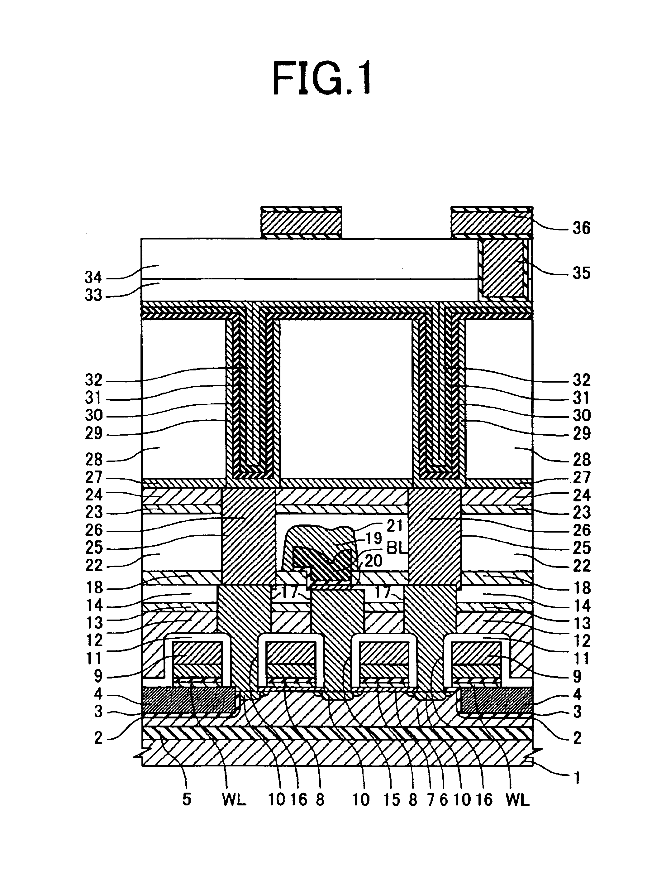
[0097]Embodiment 2 of the present invention will be described, referring to FIG. 2. This is an embodiment wherein an MIS capacitor using a dielectric film made of a layered film composed of a niobium pentoxide film and a tantalum pentoxide film is applied to a semiconductor memory device, in particular, such a DRAM.

[0098]The DRAM of the present embodiment is the same as in Embodiment 1 except differences in data-storing capacitor element structure. Accordingly, only the differences will be described hereinafter, and description on the same matters is omitted.

[0099]The process for producing the DRAM of Embodiment 2 is the same as in Embodiment 1 about the steps before the plug 26 is formed inside the through hole 25. In Embodiment 2, the plug 26 is formed by depositing a polycrystalline silicon film doped with an N-type impurity (such as P (phosphorus)) by CVD and then etching-back this polycrystalline silicon film so as to cause some parts thereof to remain inside the through hole 2...

embodiment 3

[0111]FIG. 3 is a sectional view of a MISFET which is a semiconductor device of Embodiment 3. This is an example wherein a dielectric film made of a layered film composed of a niobium pentoxide film and a tantalum pentoxide film is used as a gate insulator film of the MISFET.

[0112]First, a semiconductor substrate 101, which is the same as the semiconductor substrate 1 in Embodiment 1, is prepared, and a groove 102 of an isolation element region is made in a main face of the semiconductor substrate 101 and a silicon oxide film 103 is formed inside the groove 102. The formation of the groove 102 and the silicon oxide film 103 is performed in the same way as the formation of the groove 2 and the silicon oxide film 4 in Embodiment 1.

[0113]Next, niobium pentoxide is deposited on the whole surface of the semiconductor substrate 101, and then crystallized to form a niobium pentoxide film 104. Furthermore, a tantalum pentoxide film is deposited on the niobium pentoxide film 104, and crystal...


PUM

PropertyMeasurementUnit
Thicknessaaaaaaaaaa
Nanoscale particle sizeaaaaaaaaaa
Dielectric polarization enthalpyaaaaaaaaaa

Abstract

The present invention relates to a structure of a capacitor, in particular using niobium pentoxide, of a semiconductor capacitor memory device. Since niobium pentoxide has a low crystallization temperature of 600° C. or less, niobium pentoxide can suppress the oxidation of a bottom electrode and a barrier metal by heat treatment. However, according to heat treatment at low temperature, carbon incorporated from CVD sources into the film is not easily oxidized or removed. Therefore, a problem that leakage current increases arises. As an insulator film of a capacitor, a layered film composed of a niobium pentoxide film and a tantalum pentoxide film, or a layered film composed of niobium pentoxide films is used. By the use of the niobium pentoxide film, the dielectric constant of the capacitor can be made high and the crystallization temperature can be made low. By multiple-stage formation of the dielectric film, leakage current can be decreased.

Description

[0001]This application is a continuation of application No. 10 / 300,763 filed Nov. 21, 2002, now U.S. Pat. No. 6,833,577.BACKGROUND OF THE INVENTION[0002]1. Field of the Invention[0003]The present invention relates to a technique suitable for a semiconductor device and a process for producing the same, in particular, a semiconductor device having a capacitor, for example, a dynamic random access memory (DRAM), and a process for producing the same.[0004]2. Description of Related Art[0005]It is known that for large scale integration of semiconductor devices or other purposes, a tantalum pentoxide film having a dielectric constant of several tens is adopted instead of a silicon oxide film (dielectric constant: about 4) or a silicon nitride film (dielectric constant: about 7), which has been conventionally used as a capacitor dielectric film (for example, JP-A No. 139288 / 1998).[0006]As a process for producing a capacitor having the tantalum pentoxide dielectric film, there is known a pro...

Claims


Application Information

Patent Timeline
IPC IPC(8): C23C16/18C23C16/56C23C16/40H01L21/02H01L21/316C23C16/44H01L21/70H01L27/108H01L21/8242H01L21/314H01L27/04H01L21/822H01L21/8234H01L27/06H01L29/78
CPCC23C16/18C23C16/405C23C16/56H01L21/02175H01L21/02183H01L21/02194H01L21/022H01L21/02271H01L21/02356H01L21/31604H01L21/31637H01L28/40H01L27/10814H01L27/10852H01L27/10882H01L27/10894H01L28/56H01L28/75H01L28/90H10B12/315H10B12/033H10B12/48H10B12/09
Inventor MATSUI, YUICHIHIRATANI, MASAHIKO
Owner RENESAS ELECTRONICS CORP
Why Eureka
Try Eureka