Schottky-barrier tunneling transistor

a tunneling transistor and shielding shield technology, applied in the field of semiconductor transistor devices, can solve the problems of low sheet resistance, low dielectric constant of gate insulators, and no known solution for mos device technology to continue, and achieve the effects of reducing short channel effect, reasonable on/off current ratio, and higher gate leakage curren

Inactive Publication Date: 2005-11-08
WU KOUCHENG
View PDF6 Cites 5 Cited by
  • Summary
  • Abstract
  • Description
  • Claims
  • Application Information

AI Technical Summary

Benefits of technology

[0042]Another advantage of the present invention is that the invention SBTT device can be operated at a low power supply voltage due to its unique current conduction mechanism. The SBTT device can operate, for example, 0.4 V or below, because the current conduction mechanism is quantum mechanical tunneling. The electrons inject from the conduction band of the emitter to the conduction band of the base through the emitter-base Schottky barrier by tunneling. The power supply voltage does not need to be large enough to induce the carrier inversion as in a MOSFET. The device can be designed so that the Schottky barrier can be modulated by a small base voltage. The device simulation shows that the turn-on behavior of a SBTT is more sensitive than that of a MOSFET. On the other hand, the current conduction mechanisms are drift and diffusion in a MOSFET. For an n-channel MOSFET, the silicon surface needs to be inverted from p-type to n-type by a positive gate voltage and forms a channel to connect the source and the drain. The required gate voltage depends on the gate insulator thickness, gate insulator dielectric constant, surface doping, and the silicon band gap. The surface doping actually increases with shrinking device dimensions in order to suppress the short channel effect. The reduction of power supply voltage in the past is primarily attributed to the gate oxide thickness reduction. To have a reasonable on / off current ratio, the power supply voltage is difficult to be smaller than 0.6 V. In the last 10 years, the MOS device scaling basically follows the constant electric field scaling rules to maintain constant electric fields inside the device. For example, the average electric field between drain and source remains the same when the technology migrates from 0.5 μm (with Vdd=5 V) in 1993 to 0.1 μm (with Vdd=1 V) in 2003. In the next 10 years, according to the ITRS Roadmap, the scaling of power supply voltage is slower than the scaling of MOS device geometries. For example, the power supply voltage is only reduced to 0.6 V for the 32-nm technology in 2013, which should be 0.32 V if the constant electric field scaling rules are strictly followed. The maximum electric fields in the gate insulator and in the channel will be increased for the future small geometry devices. The higher electric fields will cause the problems of higher gate leakage current, short channel effect, hot-carrier injection, gate insulator reliability, and higher power consumption. The difficulty of scaling down the power supply voltage should eventually slow down the MOS device scaling roadmap.

Problems solved by technology

Fundamental limits in SiO2 scaling due to tunneling current, in SDE junction depths due to large increases in external resistance, and in well engineering due to leakage constraints are currently being reached.
The most apparent challenges are gate insulators with high dielectric constant and ultra-shallow junctions with low sheet resistance.
At present, there are no known solutions for the MOS device technologies to continue the performance trends seen in the last 20 years.
Practical and fundamental limits are being approached and substantial changes to device technologies and structures are required.
Aggressive scaling of silicon integrated devices in the deep sub-micron range presents considerable challenges to device engineers.

Method used


Image

  • Schottky-barrier tunneling transistor
  • Schottky-barrier tunneling transistor
  • Schottky-barrier tunneling transistor

Examples


Embodiment Construction

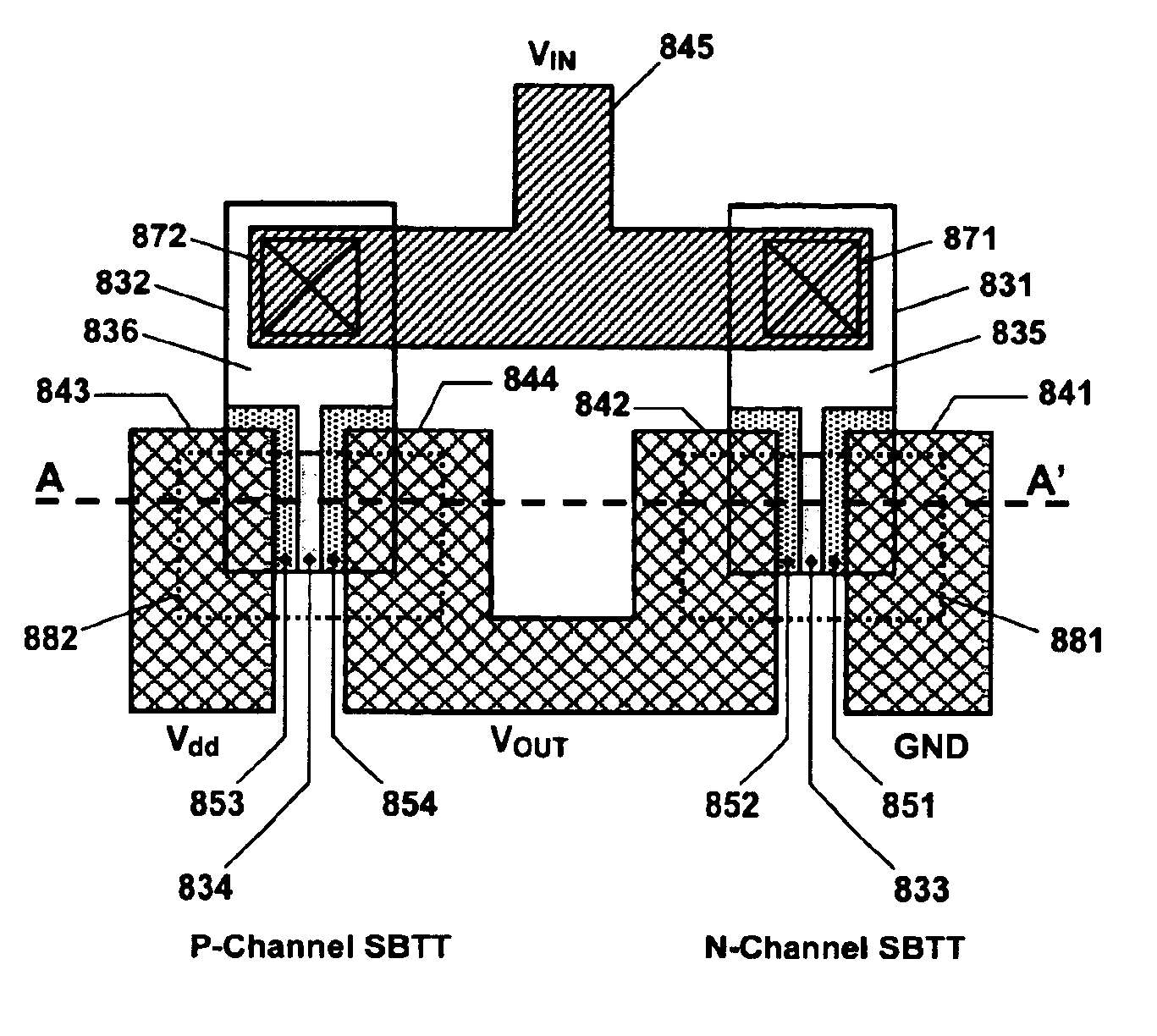
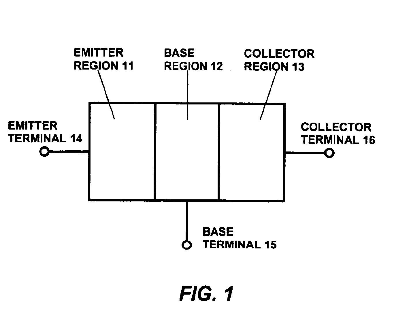
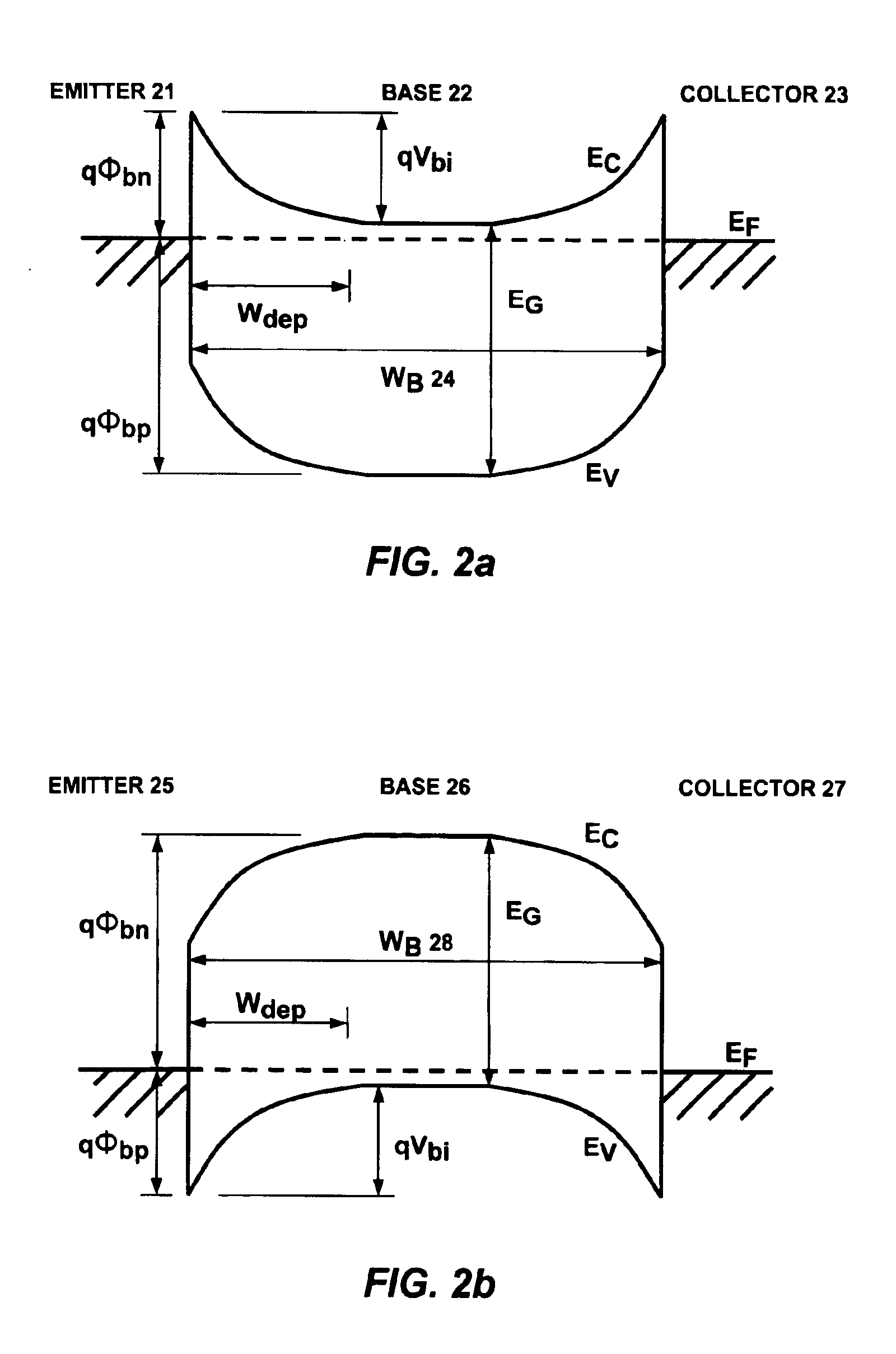
[0064]Reference will now be made in detail to the preferred embodiments of the invention, examples of which are illustrated in the accompanying drawings. While the invention will be described in conjunction with the preferred embodiments, it will be understood that they are not intended to limit the invention to these embodiments. On the contrary, the invention is intended to cover alternatives, modifications and equivalents, which may be included within the spirit and scope of the invention as defined by the appended claims. Furthermore, in the following detailed description of the present invention, numerous specific details are set forth in order to provide a thorough understanding of the present invention. However, it will be obvious to one of ordinary skill in the art that the present invention may be practiced without these specific details. In other instances, well known methods, procedures, components, and circuits have not been described in detail as not to unnecessarily ob...


PUM


Abstract

A three-terminal semiconductor transistor device comprises a base region formed by a semiconductor material of a first conductivity type at a first concentration, the base region being in contact with a first electrical terminal via a semiconductor material of the second conductivity type at a second concentration, wherein the second concentration is lower than the first concentration. The three-terminal semiconductor transistor device also includes a conductive emitter region in contact with the semiconductor base region, forming a first Schottky barrier junction at the interface of the conductive emitter region and the semiconductor base region. The conductive emitter region is in contact with a second electrical terminal. The three-terminal semiconductor transistor device further includes a conductive collector region in contact with the semiconductor base region, which forms a second Schottky barrier junction at the interface of the conductive collector region and the semiconductor base region. The conductive collector region is in contact with a third electrical terminal. The tunneling current through the first Schottky barrier junction or the second Schottky barrier junction is substantially controlled by the voltage of the semiconductor base region.

Description

RELATED APPLICATIONS[0001]This application is a Continuation-in-Part of the U.S. patent application Ser. No. 10 / 438,674, filed on May 15, 2003, now U.S. Pat. No. 6,744,111 titled “Schottky-Barrier Tunneling Transistor”, the content of which is hereby incorporated by reference.TECHNICAL FIELD[0002]This application relates to a semiconductor device, specifically, a semiconductor transistor device suitable for analog and digital circuits.BACKGROUND OF THE INVENTION[0003]For more than 30 years, the integrated circuit industry has followed a dramatic path of shrinking device dimensions and increasing chip sizes, resulting in steadily increased performance and increased functionality. New generations of devices have appeared in every two to three years, following the so called “Moore's Law”, with each new generation device approximately doubling logic circuit density, increasing performance by about 40%, and quadrupling the memory capacity comparing to the previous generation. The consist...

Claims


Application Information

Patent Timeline
Patent Type & Authority Patents(United States)
IPC IPC(8): H01L21/70H01L27/12H01L21/84H01L27/095H01L29/47H01L29/812H01L31/07
CPCH01L21/84H01L27/1203
Inventor WU, KOUCHENG
Owner WU KOUCHENG
Why Eureka
Try Eureka