Siloxane epoxy polymers for low-k dielectric applications

a technology of epoxy polymers and dielectrics, applied in the field of dielectric materials, can solve the problems of limiting circuit speed, unable to meet the needs of the semiconductor industry, and reducing the ic frequency, so as to achieve better performan

Active Publication Date: 2006-03-28
POLYSET +1
View PDF5 Cites 10 Cited by
  • Summary
  • Abstract
  • Description
  • Claims
  • Application Information

AI Technical Summary

Benefits of technology

[0007]The present invention meets the aforementioned needs and unexpectedly provides for semiconductor devices that utilize new low-κ dielectric polymeric materials therein, particularly as interlayer dielectrics between metallization levels. In particular, the siloxane epoxy polymers described herein have dielectric constants (κ values) lower than 3, and as low as 1.8 under certain processing conditions. Thus the devices utilizing such materials can provide much better performance than devices fabricated using conventional dielectric materials, such as SiO2, for example. Advantageously, the siloxane epoxy polymer materials can be fully cured at temperatures as low as 155° C., while retaining their stability and dielectric properties at high semiconductor device processing temperatures greater than 400° C.

Problems solved by technology

The higher the value of the R times C product, the more limiting the circuit speed.
With the continued shrinking of semiconductor devices, high resistance-capacitance (RC) delay has become a major hindrance to the further increase of the IC frequency.
Currently available low κ polymeric dielectric materials require high processing temperatures of >350° C., and are thus not best suited to meet the needs of the semiconductor industry.

Method used


Image

  • Siloxane epoxy polymers for low-k dielectric applications
  • Siloxane epoxy polymers for low-k dielectric applications
  • Siloxane epoxy polymers for low-k dielectric applications

Examples


example 1

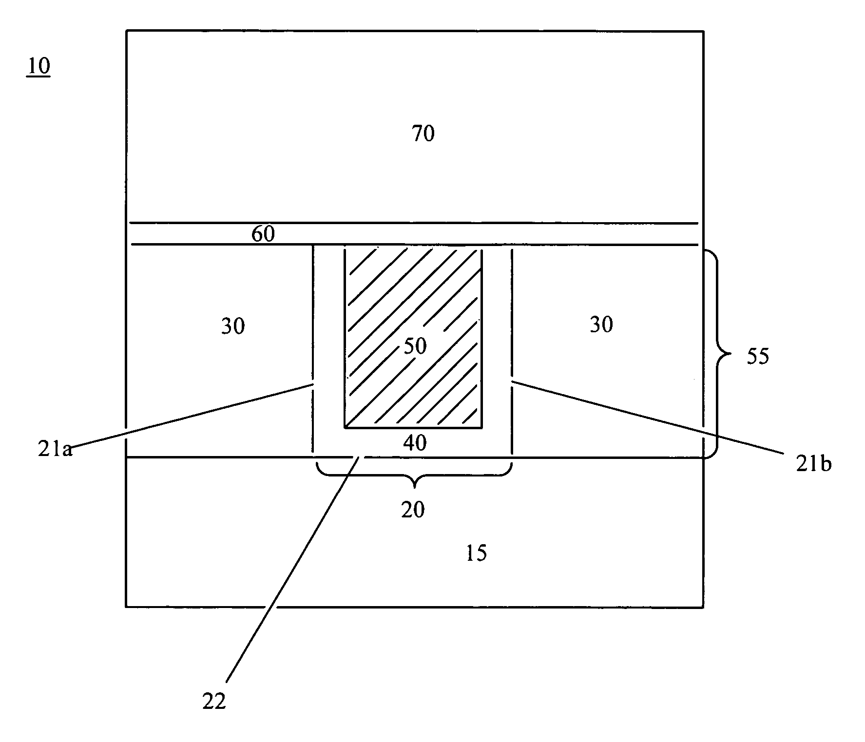
[0038]N-type, 4-inch silicon wafers having a resistivity of 0–0.02 ohm-cm for MIM (Metal-Insulator-Metal) structures were used as the semiconductor substrates. After standard RCA cleaning an adhesion promoter (HMDS) was spin-coated onto each wafer at 3000 rpm for 40 sec. The wafers were then annealed in air at 100° C. for 10 min. A siloxane epoxy polymer solution containing formula (IIB), wherein the ratio of p to q was about 2:1, was spin-coated onto each wafer at 3000 rpm for 100 sec to a thickness of 0.5 μm. The polymeric film / wafers were dried under vacuum of 10−3 torr for 1 hour at 100° C. The polymer films were then cured at 165° C. under nitrogen gas flow for 2 hours to cross-link the polymer.

example 2

[0039]The procedure of Example 1 was followed. After curing, the polymer films were subjected to a thermal anneal at 250° C. under nitrogen gas flow for 2 hours.

[0040]The dielectric constants of the polymer films from Examples 1 and 2 were determined by measuring the capacitance of the polymer films (i.e., Metal-Insulator-Semiconductor (MIS) capacitor devices, Metal-Insulator-Metal (MIM) capacitor devices, and C-V techniques). The polymer was regularly shown to have a dielectric constant below 2.65. However, a dielectric constant as low as 2.2 has been measured for thinner films ranging from about 0.02 μm to about 0.09 μm.

example 3

[0041]Metal-Insulator-Semiconductor (MIS) capacitor structures were prepared from the samples of Example 1 by depositing a copper metal film directly onto the polymer layer of each sample prior to drying and curing. Copper served as an electrode in the structures. The copper metal thin films were deposited to a thickness of 0.3 μm using sputtering or e-beam evaporation. After drying and curing, as described in Example 1, the samples were then annealed at 250° C. under nitrogen gas for 1 hr.

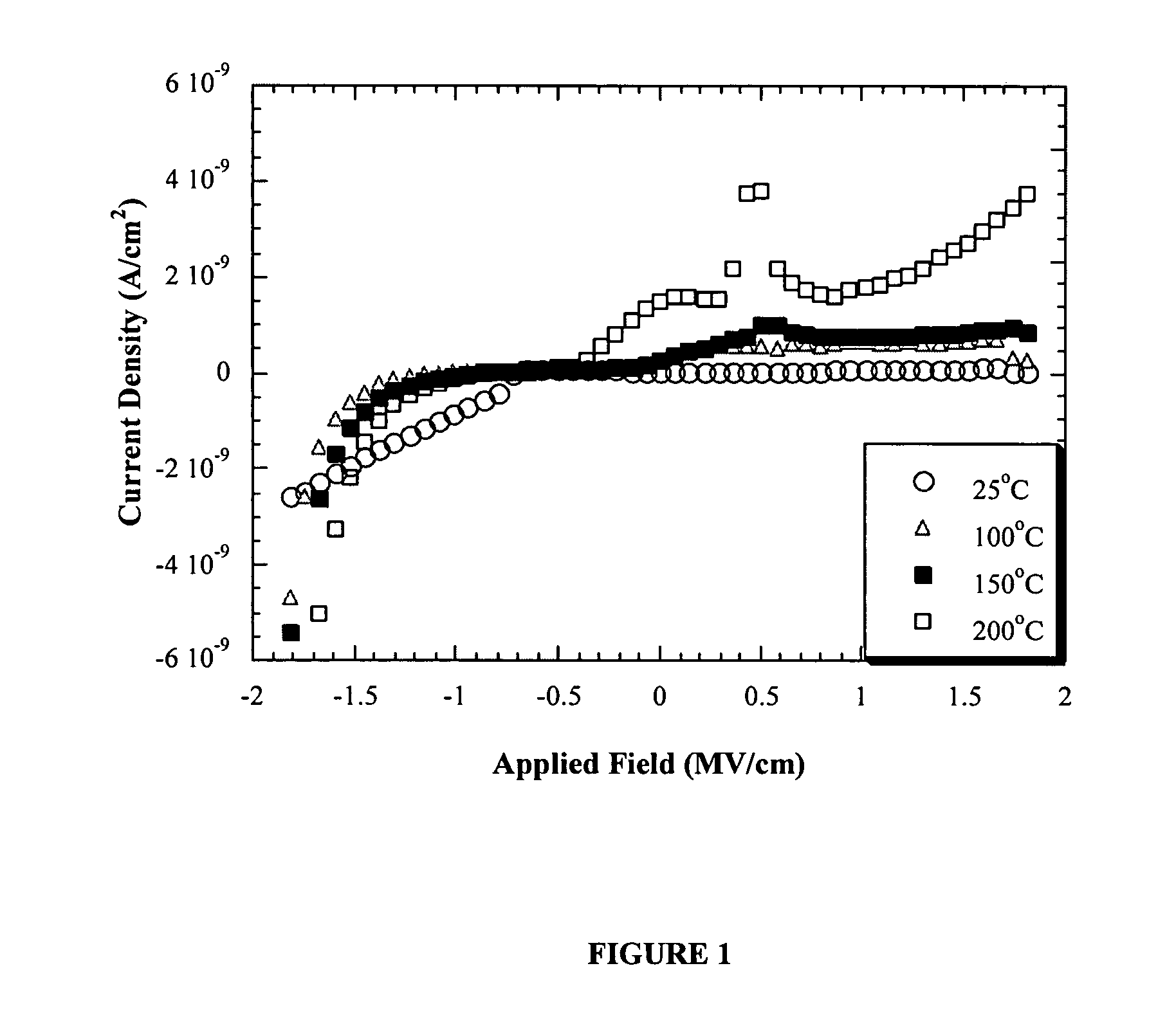
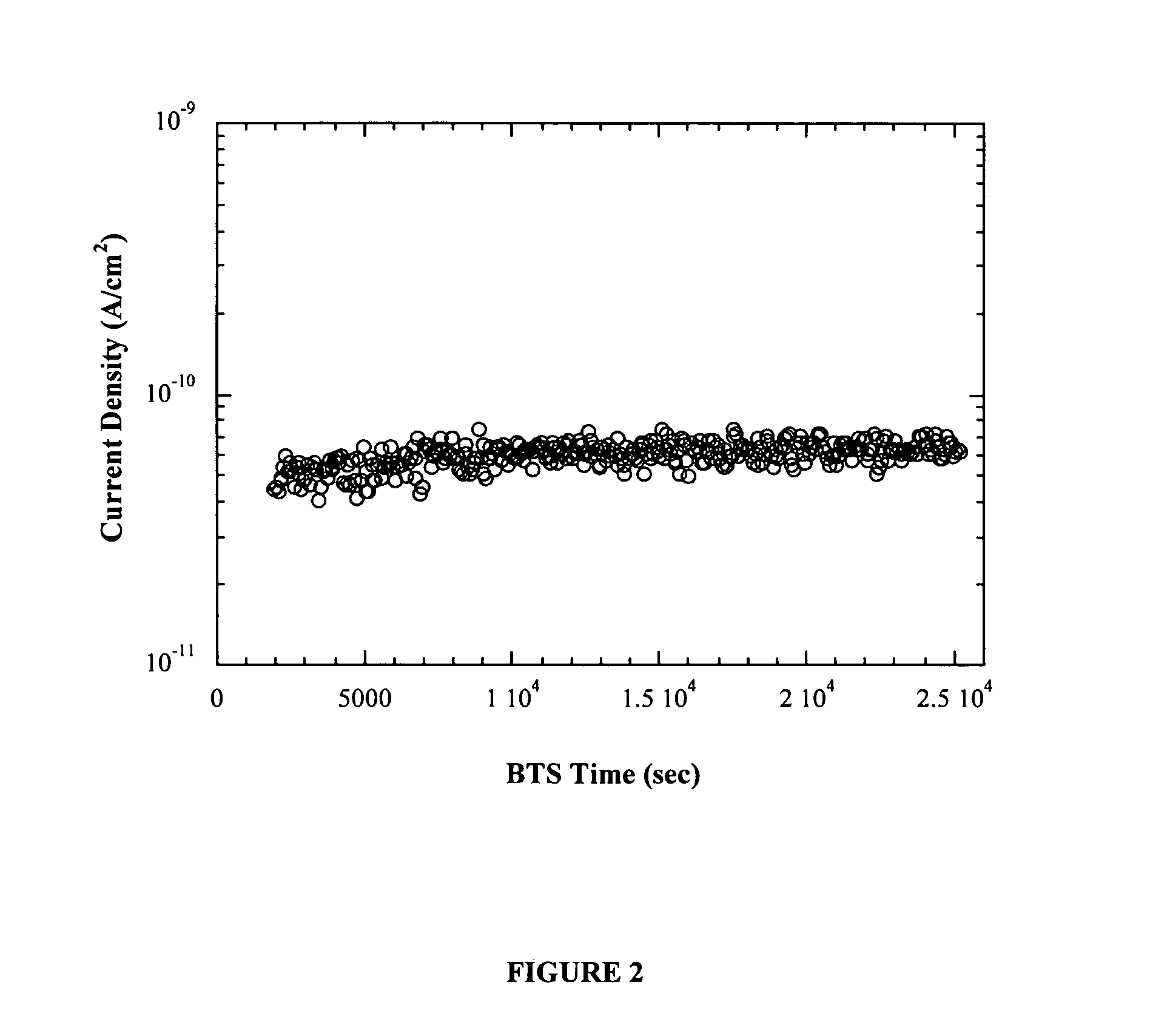
[0042]The electrical stability of the siloxane epoxy polymer (IIB) used in the capacitors of Example 3 was examined by doing I–V measurements on the films at 25° C. and higher temperatures. The measured current (I) was divided by the electrode area to get current density (J), and the voltage (V) was divided by the film thickness (0.5 μm) to get applied electrical field (E). The J (A / cm2) vs. E (MV / cm) plot for the polymer is shown in FIG. 1 and indicates that the leakage current density through th...


PUM

PropertyMeasurementUnit
thicknessaaaaaaaaaa
thicknessaaaaaaaaaa
temperaturesaaaaaaaaaa

Abstract

Semiconductor devices employing siloxane epoxy polymers as low-κ dielectric films are disclosed. The devices include a semiconductor substrate, one or more metal layers or structures and one or more dielectric films, wherein at least one dielectric film in the devices is a siloxane epoxy polymer. Use of siloxane epoxy polymers is advantageous, in part, because the polymers adhere well to metals and have dielectric constants as low as 1.8. Thus, the disclosed semiconductor devices offer much better performance than devices fabricated using conventional dielectric materials. Furthermore, the siloxane epoxy polymer dielectrics are fully curable at low temperatures, exhibit low leakage currents, and remain stable at temperatures greater than 400° C. making them particularly attractive for use in the semiconductor industry

Description

CROSS-REFERENCE TO RELATED APPLICATIONS[0001]This Application is related to the following copending U.S. Patent Applications:[0002]U.S. patent application Ser. No. 10 / 832,629, filed Apr. 27, 2004, entitled “CHEMICAL TREATMENT OF MATERIAL SURFACES”; and U.S. patent application Ser. No. 10 / 832,844, filed Apr. 27, 2004, entitled “SILOXANE EPOXY POLYMERS AS METAL DIFFUSION BARRIERS TO REDUCE ELECTROMIGRATION”.Each of these Applications is hereby incorporated by reference herein in its entirety.FIELD OF THE INVENTION[0003]The present invention relates to dielectric materials employed in semiconductor devices, and more particularly to siloxane epoxy polymers useful as low-κ dielectric materials in such devices.BACKGROUND OF THE INVENTION[0004]The speed of semiconductor circuitry varies inversely with the resistance (R) and capacitance (C) of the interconnection system. The higher the value of the R times C product, the more limiting the circuit speed. With the continued shrinking of semic...

Claims


Application Information

Patent Timeline
Patent Type & Authority Patents(United States)
IPC IPC(8): H01L23/58C08G77/04C09D183/06H01L23/532
CPCC09D183/06H01L23/5329H01L2924/12044H01L23/53238H01L2924/0002H01L2924/00
Inventor GHOSHAL, RAMKRISHNAWANG, PEI-ILU, TOH-MINGMURARKA, SHYAM P.
Owner POLYSET
Why Eureka
Try Eureka