Surface processing method of a specimen and surface processing apparatus of the specimen
- Summary
- Abstract
- Description
- Claims
- Application Information
AI Technical Summary
Benefits of technology
Problems solved by technology
Method used
Image

Examples
embodiment 1
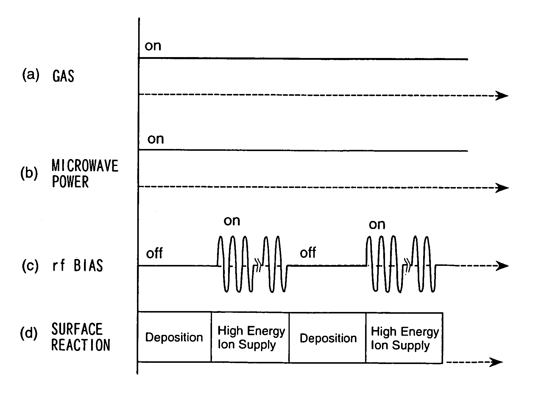
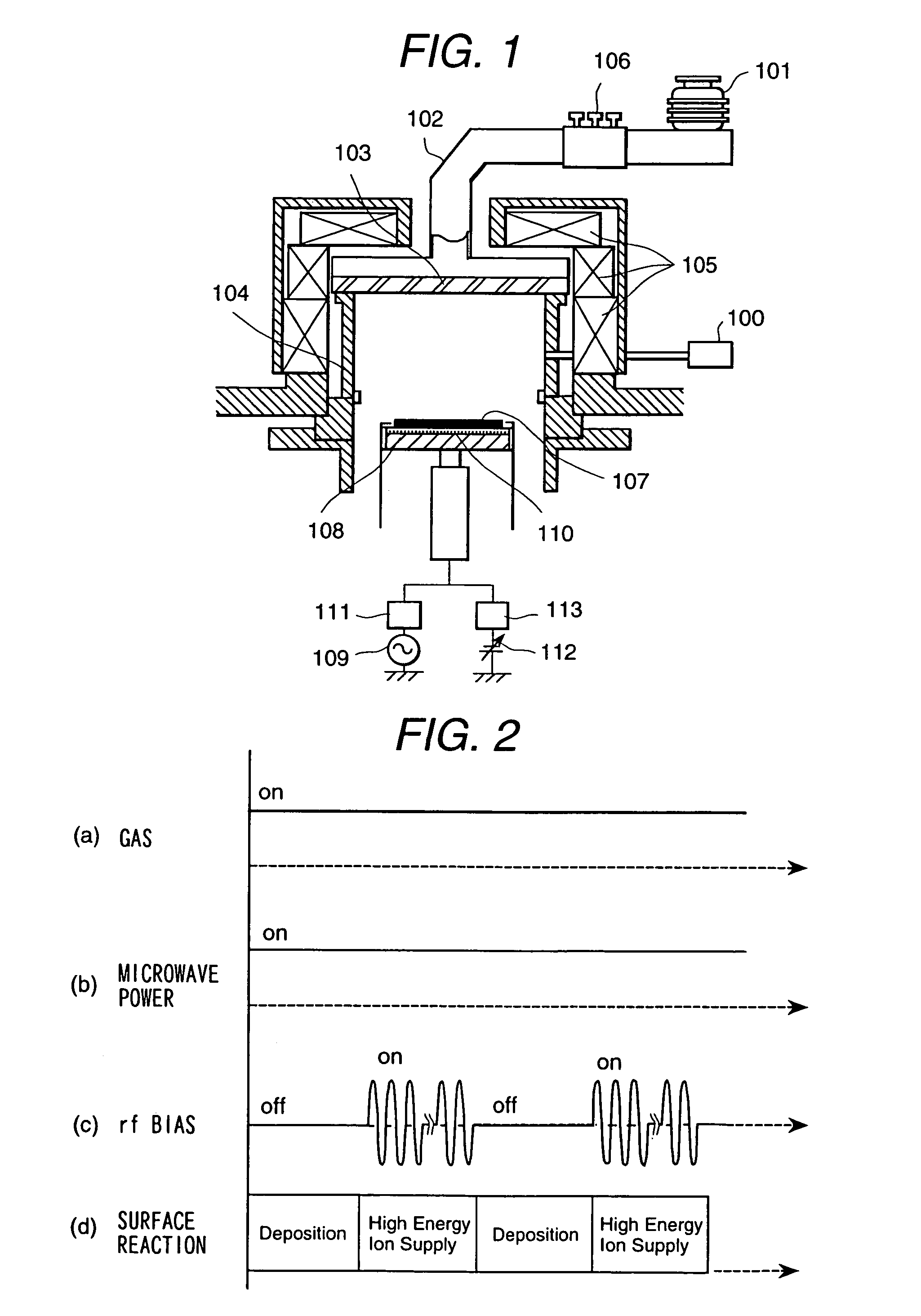
[0034]With reference to FIG. 1 to FIG. 12, a first embodiment of the invention will be described in the following.
[0035]FIG. 1 is a diagram showing a plasma etcher to which the invention is applied. Microwaves are introduced from a magnetron 101 via an automatic matching apparatus 106, a waveguide 102, and a transparent window 103 into a chamber 104. Meanwhile, an etching gas, such as a halogen gas, is introduced into the chamber 104 via a gas introducing means 100, and a plasma of the gas is generated in the chamber 104 in association with the introduction of the microwaves. The transparent window 103 is made of a material, such as quartz and ceramics, which is able to transmit microwaves (electromagnetic waves).
[0036]Around the chamber 104, coils 105 are arranged. The magnetic flux density of the coils 105 is set so as to resonate with the frequency of the microwaves. For example, when the frequency is 2.45 GHz, the magnetic flux density is 875 Gauss. With the magnetic flux densit...
embodiment 2
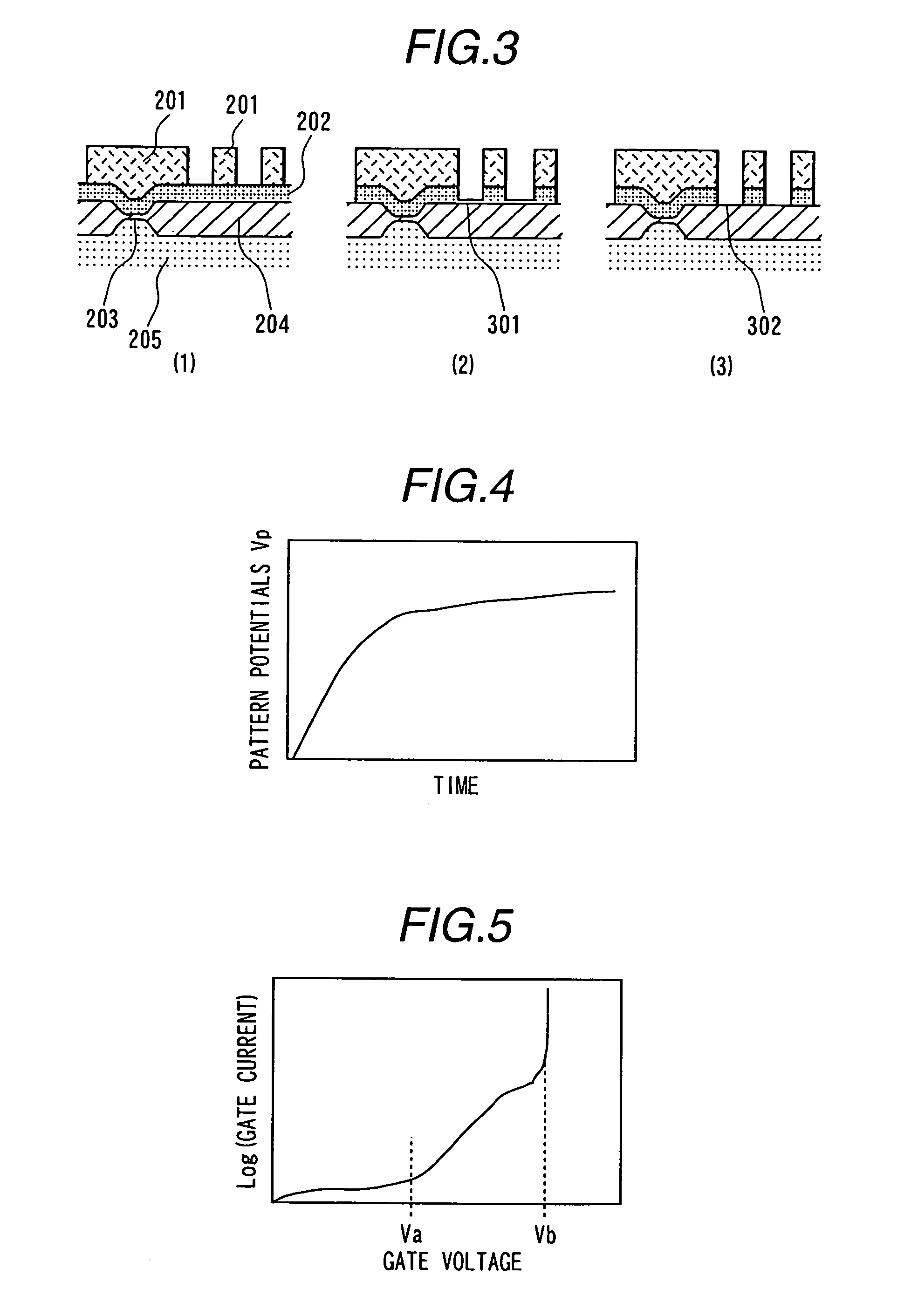
[0060]FIG. 13 shows a construction of an apparatus according to another embodiment of the invention, wherein a plasma is generated by induction coupling using so-called radio wave band frequencies in a range from several hundred kHz to several tens MHz (referred to as rf hereinafter). Vacuum chamber 1303 is made of a material such as alumina, quartz or the like which allows electromagnetic waves to pass. An electromagnetic coil 1302 is wound around the chamber for generating plasma 1310. An rf power supply 1304 is connected to the coil. A specimen table 1308 is placed within the vacuum chamber 1301, on which a specimen 1307 is mounted. A high frequency voltage supply 1309 is connected to the table. An upper cover 1305 is attached to vacuum chamber 1301, which may be provided integral therewith.
[0061]In this apparatus according to the second embodiment of the invention, if an increase in the pattern potentials is suppressed by repetitively turning on and off the high frequency voltag...
embodiment 3
[0063]FIG. 14 shows a construction of an apparatus according to still another embodiment of the invention, wherein a plasma is generated by capacitance coupling of rf power. In its vacuum chamber 1401, two sheets of electrodes 1402 and 1405 are placed in parallel. An rf power supply 1403 and a high frequency voltage power supply 1406 are connected to these electrodes, respectively. A specimen 1404 is mounted on the electrode 1405 which serves also as a specimen table. A gas is introduced into the chamber from an inlet pipe 1408 through openings provided in the electrode 1404 opposite to the specimen. A plasma 1407 is generated in a space between the two sheets of electrodes.
[0064]In this apparatus according to the invention, by suppressing an increase in the pattern potentials by repetitively turning on and off the high frequency voltage supply 1406 in the same manner as described above, breakdown of the gate oxide film can be prevented.
[0065]According to the invention as described ...
PUM
 Abstract
Description
Claims
Application Information
 - R&D
- Intellectual Property
- Life Sciences
- Materials
- Tech Scout
- Unparalleled Data Quality
- Higher Quality Content
- 60% Fewer Hallucinations
Browse by: Latest US Patents, China's latest patents, Technical Efficacy Thesaurus, Application Domain, Technology Topic, Popular Technical Reports.
© 2025 PatSnap. All rights reserved.Legal|Privacy policy|Modern Slavery Act Transparency Statement|Sitemap|About US| Contact US: help@patsnap.com