Dielectric film structure, piezoelectric actuator using dielectric element film structure and ink jet head

a film structure and dielectric element technology, applied in the field of dielectric film structure, piezoelectric actuator using dielectric element film structure and ink jet head, can solve the problems of increased number, increased length of ink jet head, increased number of dielectric films obtained by screen printing, etc., to achieve excellent piezoelectric, pyroelectric and ferroelectric properties, excellent dielectric properties and endurance, and excellent piezoelectric properties.

Inactive Publication Date: 2006-06-13
CANON KK
View PDF18 Cites 28 Cited by
  • Summary
  • Abstract
  • Description
  • Claims
  • Application Information

AI Technical Summary

Benefits of technology

[0060]Since such a dielectric film structure of the present invention has the excellent dielectric, piezoelectric, pyroelectric and ferroelectric properties, compactness and a high integrating ability of an element such as an actuator, a memory and a sensor can be achieved.
[0061]Further, the piezoelectric actuator of the present invention has both excellent piezoelectri...

Problems solved by technology

However, in consideration of development of high density of nozzle arrangement and lengthening of the ink jet head (increase in the number of nozzles per one head), the method using the screen printing has the following problems.
Accordingly, in order to achieve higher density of the nozzle arrangement, the dielectric film obtained by the screen printing may not provide a satisfactory piezoelectric property.
Such positional deviation of the dielectric film may cause a great problem regarding influence upon a discharging property as higher density of the nozzle arrangement is achieved and the length of the ink jet head is increased.
Further, in general, although minute working of a silicon substrate using a semiconductor manufacturing technique is considered to be bright...

Method used


Image

  • Dielectric film structure, piezoelectric actuator using dielectric element film structure and ink jet head
  • Dielectric film structure, piezoelectric actuator using dielectric element film structure and ink jet head
  • Dielectric film structure, piezoelectric actuator using dielectric element film structure and ink jet head

Examples


embodiments 1 to 5

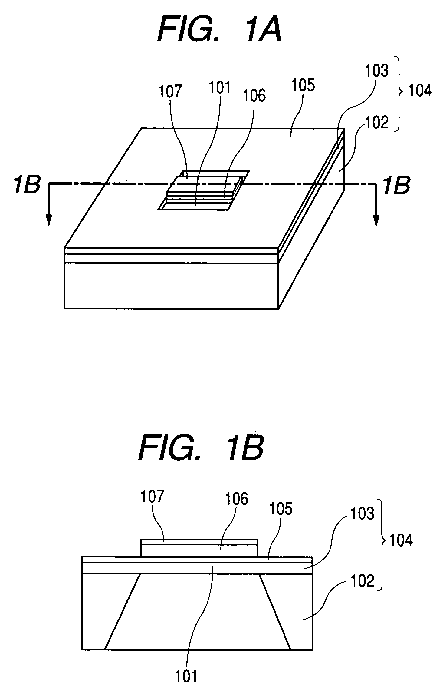
[0082]As the dielectric film structures for embodiments 1 to 5, a piezoelectric actuator of both-lever type shown in FIGS. 1A and 1B was manufactured. FIG. 1A is a perspective view of the piezoelectric actuator of both-lever type according to the present invention and FIG. 1B is a sectional view taken along the line 1B—1B in FIG. 1A. Regarding a dimension of a beam (lever) 101, a width is 100 μm and a length is 800 μm.

[0083]First of all, a mask was provided on a (100) silicon substrate 102 so that a pattern of the beams can be formed and strontium titanate having (100) face orientation and having a thickness of 700 nm to 4000 nm was film-formed by a spattering method, thereby obtaining a vibrating plate 103. The reference numeral 104 indicates a substrate of the dielectric film structure of the present invention. A mask was similarly provided on this substrate and platinum having (100) face orientation was epitaxial-grown by a spattering method, thereby forming a lower electrode 105...

embodiment 6

[0091]A lower electrode was formed by epitaxial-growing platinum having (100) face orientation and a thickness of 10 nm on a (100) substrate of strontium titanate by means of a spattering method. Lead titanate zirconate having a thickness of 10 nm and (100) face orientation was epitaxial-grown on the lower electrode by an RF magnetron spattering method under the above-mentioned condition, thereby forming a dielectric film having a thickness of 10 nm. Film thicknesses of the dielectric film, element ratios between zirconium and titanium and a result of the X ray diffraction measurement are shown in the following Table 5. Platinum having a thickness of 10 nm was film-formed on the dielectric film by a spattering method thereby to form an upper electrode, thereby completing a dielectric film structure. An endurance test was performed by using such a dielectric film structure. Voltage was applied up to maximum voltage of 1V. However, leak was not generated and there is no problem regard...

embodiment 7

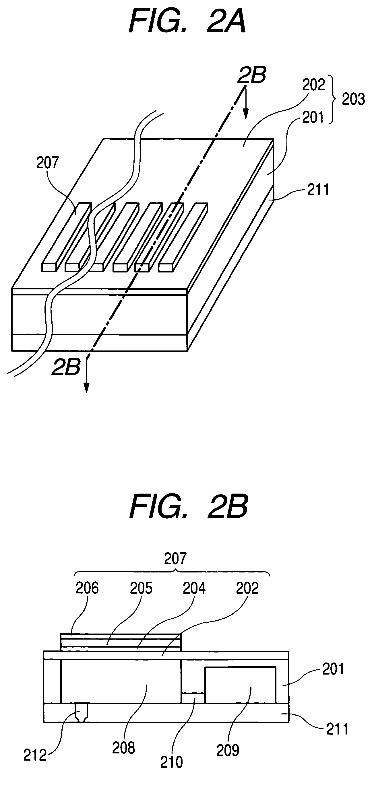
[0092]An ink jet head shown in FIGS. 2A and 2B was manufactured as follows. FIG. 2A is a perspective view showing an example of an ink jet head of the present invention and FIG. 2B is a sectional view taken along the line 2B—2B in FIG. 2A.

[0093]A strontium titanate layer having (100) face orientation and a thickness of about 2000 nm was film-formed on a (100) silicon substrate constituting a flow path substrate 201, thereby forming a vibrating plate 202. This plate was used as a substrate 203 of the dielectric film structure of the present invention. A mask was patterned on the strontium titanate layer in correspondence to positions where ink pressurizing chambers 208 are to be formed and platinum having (100) face orientation was epitaxial-grown by a spattering method, thereby forming a lower electrode 204 having a thickness of about 100 nm. A mask having a width of 100 μm and a length of 5 mm was patterned on the lower electrode 204 and a dielectric film 205 of 0.9 PZT-0.1 PMN sol...


PUM


Abstract

The present invention provides a dielectric film structure having a substrate and a dielectric film provided on the substrate and in which the dielectric film has (001) face orientation with respect to the substrate, and in which a value u in the following equation (1) regarding the dielectric film is a real number greater than 2:
u=(Cc/Ca)×(Wa/Wc)  (1)
where, Cc is a count number of a peak of a (00l′) face of the dielectric film in an Out-of-plane X ray diffraction measurement (here, l′ is a natural number selected so that Cc becomes maximum); Ca is a count number of a peak of a (h′00) face of the dielectric film in an In-plane X ray diffraction measurement (here, h′ is a natural number selected so that Cc becomes maximum); Wc is a half-value width of a peak of the (00l′) face of the dielectric film in an Out-of-plane rocking curve X ray diffraction measurement; and Wa is a half-value width of a peak of the (h′00) face of the dielectric film in an In-plane rocking curve X ray diffraction measurement.

Description

BACKGROUND OF THE INVENTION[0001]1. Field of the Invention[0002]The present invention relates to a dielectric film structure having excellent dielectric property, piezoelectric property, pyroelectric property and ferroelectric property and available as an element such as an actuator, a memory or a sensor. Further, the present invention relates to a piezoelectric actuator having such a dielectric film structure. Furthermore, the present invention relates to an ink jet head utilizing such a piezoelectric actuator as a discharge pressure generating element for discharging liquid.[0003]2. Related Background Art[0004]Presently, a dielectric film structure having a dielectric film including solid solution of lead titanate zirconate (Pb(Zr, Ti)O3, PZT), barium titanate (BaTiO3), lead titanate zirconate—lead magnesium niobate (Pb(Zr, Ti)O3—Pb(Mg1 / 3Nb2 / 3)O3, PZT-PMN) has widely been used various elements such as actuators, memories and sensors by utilizing dielectric, piezoelectric, pyroelec...

Claims


Application Information

Patent Timeline
IPC IPC(8): B41J2/045B41J2/055B41J2/135B41J2/14H01B3/12H01L29/00H01L41/08H01L41/09H01L41/18H01L41/187H01L41/22H01L41/316
CPCB41J2/14233H01L41/0973H01L41/314H10N30/2047H10N30/076H10N30/00
Inventor AOTO, HIROSHITAKEDA, KENICHIFUKUI, TETSUROIFUKU, TOSHIHIRO
Owner CANON KK
Why Eureka
Try Eureka