Thin film device provided with coating film, liquid crystal panel and electronic device, and method for making the thin film device

a thin film, liquid crystal panel technology, applied in the direction of optics, instruments, transportation and packaging, etc., can solve the problems of low uniformity of film thickness, large dependence on tft substrate cost, and high proportion of the cost of liquid crystal display devices. achieve the effect of high throughpu

Inactive Publication Date: 2006-06-27
SEIKO EPSON CORP
View PDF153 Cites 27 Cited by
  • Summary
  • Abstract
  • Description
  • Claims
  • Application Information

AI Technical Summary

Benefits of technology

[0029]In the present invention, an insulating layer and a conductive layer composing a thin film monolithic structure are formed of a coating film other than the SOG film, and the thin film can be planarized at the same time. Because the coating film can be formed without a vacuum system such as a CVD system or a sputtering system, a mass-production line can be constructed with a significantly smaller investment compared to conventional systems, the throughput of the system can be increased, and the cost of the thin film device can be drastically reduced.
[0086]As described above, in accordance with the present invention, a part or all of the thin films can be formed by applying and annealing a solution, hence a thin film device can be produced with an inexpensive production unit having a high throughput.

Problems solved by technology

A part of driving circuits may be formed on the TFT substrate 60 by forming the active elements with the TFTs, and in this case, the cost of the TFT substrate represents a high proportion of the cost of the liquid crystal display device.
The cost of the TFT greatly depends on the production cost of the thin film monolithic structure.
The insulation layer in the thin film monolithic structure is formed by a low pressure chemical vapor deposition (LPCVD) process or a plasma enhanced CVD (PECVD) process, because a normal pressure CVD (NPCVD) process results in low uniformity of the film thickness.
The CVD systems and the sputtering system used in the above-mentioned film deposition processes belong to vacuum units for processing materials under vacuum pressures, and require large vacuum systems, resulting in an increase in initial investment.
The substrate atmosphere therefore must be changed from open air to vacuum, and this limits the throughput.
Because the ion implanter and the ion-doping system are also vacuum systems, the same problems as above occur.
Further, the ion implanter and the ion-doping system require complex mechanisms for generating plasma, extracting ions, mass-separating the ions (for the ion implanter), accelerating ions, collimating ions, scanning ions and so on, resulting in a remarkably high initial investment cost.
Scaling-up of the substrate size for producing large liquid crystal display devices with reduced costs is an obstacle to high speed transfer of the substrates in the vacuum system, and causes breakage of the substrate due to thermal stress during the deposition steps, hence it is significantly difficult to improve the throughput of the film deposition system.
Also, the scaling-up of the substrate size inevitably requires scaling-up of the film deposition system.
An increased cost accompanied by the increased volume in the vacuum system further increases the initial investment, and as a result, it is difficult to achieve drastic cost reduction.
Although an increased yield is a valuable means for cost reduction, a yield near the limit has been achieved, and thus drastic cost reduction is difficult in view of the yield.
This is a factor in the increased cost of thin film device production.
Regarding the resist-coating step in the photolithographic process, only less than 1% of the resist solution dropped onto the substrate remains on the substrate as the resist film after spin coating, reducing the efficiency of the use of the resist solution.
Although a printing process has been proposed as a low cost process instead of a large scale exposure system used in the exposure step, it has not yet reached practical use due to problems such as processing accuracy.
As described above, it is not possible to drastically reduce the cost of the TFT substrate, although the market requires drastic price reduction of the liquid crystal display devices.

Method used


Image

  • Thin film device provided with coating film, liquid crystal panel and electronic device, and method for making the thin film device
  • Thin film device provided with coating film, liquid crystal panel and electronic device, and method for making the thin film device
  • Thin film device provided with coating film, liquid crystal panel and electronic device, and method for making the thin film device

Examples


first embodiment

[0132](Illustration of Thin Film Device Structure)

[0133]Two examples of thin film devices including TFTs are shown in FIGS. 3 and 4.

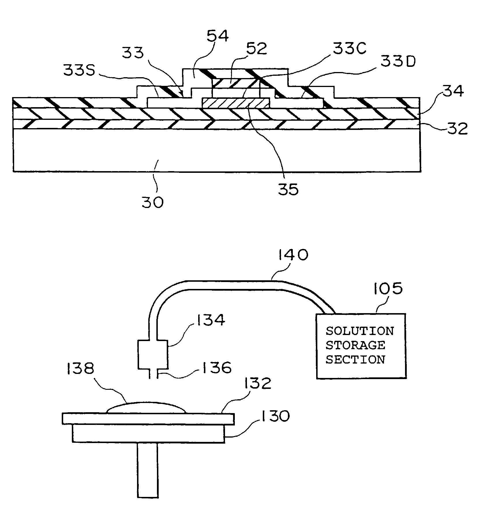
[0134]FIG. 3 is a cross-sectional view of a TFT using a coplanar-type polycrystalline silicon. An insulating underlayer 12 is formed on a glass substrate, and a polycrystalline silicon TFT is formed thereon. In FIG. 3, the polycrystalline silicon layer 14 comprises a source region 14S and a drain region 14D which are highly doped with an impurity, and a channel region 14C therebetween.

[0135]A gate insulating film 16 is formed on the polycrystalline silicon layer 14 and a gate electrode 18 and a gate line (not shown in the drawing) are formed thereon. A pixel electrode 22 composed of a transparent electrode film is connected to the drain region 14D through an opening section formed in an interlevel insulating film 20 and the gate insulating film 16 thereunder, and a source line 24 is connected to the source region 14S. A topmost protective film 26 may be...

second embodiment

[0216]FIG. 18 is an enlarged partial plan view of pixel regions formed on an active matrix substrate for a liquid crystal display device, and FIG. 19 is a cross-sectional view taken along section I–I′ of FIG. 18.

[0217]In FIGS. 18 and 19, the active matrix substrate 400 for the liquid crystal display device is divided into a plurality of pixel regions 402 by data lines Sn, Sn+1 . . . and scanning lines Gm, Gm+1 . . . on an insulating substrate 410, and each of the pixel regions 402 is provided with a TFT 404. The TFT 404 is provided with a channel region 417 forming a channel between a source region 414 and a drain region 416, a gate electrode 415 opposing to the channel region 417 with a gate insulating film 413 formed therebetween, an interlevel insulating film 421 formed on the top face of the gate electrode 415, a source electrode 431 electrically connected to the source region 414 through a contact hole 421A formed in the interlevel insulating film 421, and a pixel electrode 441...

third embodiment

[0233]FIG. 22 is an enlarged partial plan view of pixel regions formed on an active matrix substrate for a liquid crystal display device, and FIG. 23 is a cross-sectional view taken along section II–II′ of FIG. 22.

[0234]In FIGS. 22 and 23, differences between the thin film device configuration on the active matrix substrate 401 for the liquid crystal display device in accordance with the Third Embodiment and the thin film device configuration on the active matrix substrate 400 for the liquid crystal display device in accordance with the Second Embodiment are as follows.

[0235]The Third Embodiment employs a double-layer-structure interlevel insulating film including a lower interlevel insulating film 421 formed on a gate electrode 415 and an upper interlevel insulating film 422 formed on the lower interlevel insulating film 421. A source electrode 431 is therefore formed on the lower interlevel insulating film 421 and is electrically connected to a source region 414 through a contact ...


PUM

PropertyMeasurementUnit
thicknessaaaaaaaaaa
temperatureaaaaaaaaaa

Abstract

Any one of an insulating film forming a TFT, a silicon film and a conductive film is formed by applying a solution and annealing it. In a spin coater (102), a coating solution containing a thin film component which is supplied from a solution storage section (105) is spin-coated onto a substrate. The substrate after coating the coating solution is annealed in an annealing section (103) to form a coating film on the substrate. Additional laser annealing improves one of film characteristics, i.e., crystallinity, density and adhesiveness. Application of the coating solution or a resist by an ink jet process increases utilization of the solution and permits forming a patterned coating film. Because a thin film device in accordance with the present invention is inexpensive and has a high throughput, TFT production by a production system having high utilization of the coating solution drastically reduces initial investment and production cost of a liquid crystal display device.

Description

[0001]This is a Continuation of application Ser. No. 09 / 325,567 filed Jun. 4, 1999, which in turn is a Continuation of application Ser. No. 08 / 983,036 filed Feb. 13, 1998. The entire disclosure of the prior applications is hereby incorporated by reference herein in its entirety.TECHNICAL FIELD[0002]The present invention relates to a thin film device including a thin film laminate structure such as a thin film transistor (hereinafter referred to as TFT) and a method for making the same, and in particular relates to a thin film device capable of low cost production due to a decreased initial investment and a method for making the same. Also, the present invention relates to a liquid crystal panel and an electronic device using the thin film device.BACKGROUND ART[0003]In recent years, liquid crystal display devices using such types of thin film devices have been used in notebook-type personal computers, car navigation systems, video cameras and various portable information devices, and...

Claims


Application Information

Patent Timeline
Patent Type & Authority Patents(United States)
IPC IPC(8): H01L21/84G02F1/1368G02F1/1333G02F1/1362H01L21/20H01L21/205H01L21/225H01L21/288H01L21/31H01L21/3205H01L21/336H01L21/768H01L21/77H01L27/12H01L29/786
CPCG02F1/136227H01L27/12H01L29/66757H01L27/1285H01L27/1292H01L29/66765Y10T428/1064C09K2323/051Y10T428/31663H01L27/1214
Inventor YUDASAKA, ICHIOSHIMODA, TATSUYAKANBE, SADAOMIYAZAWA, WAKAO
Owner SEIKO EPSON CORP
Why Eureka
Try Eureka